166
7647H–AVR–03/12
Atmel ATmega16/32/64/M1/C1
15.2.6 SPI Data Register – SPDR
• Bits 7:0 - SPD7:0: SPI Data
The SPI Data Register is a read/write register used for data transfer between the Register File
and the SPI Shift Register. Writing to the register initiates data transmission. Reading the regis-
ter causes the Shift Register Receive buffer to be read.
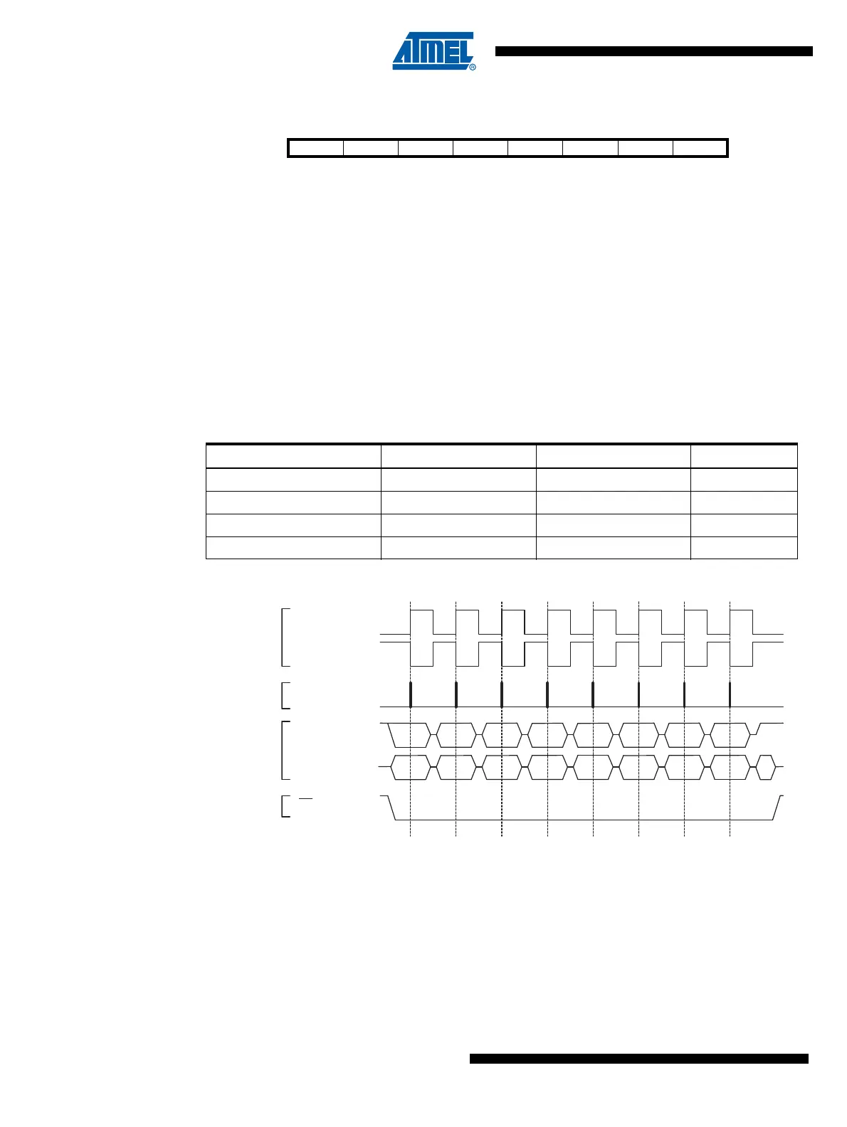
15.3 Data Modes
There are four combinations of SCK phase and polarity with respect to serial data, which are
determined by control bits CPHA and CPOL. The SPI data transfer formats are shown in Figure
15-3 and Figure 15-4. Data bits are shifted out and latched in on opposite edges of the SCK sig-
nal, ensuring sufficient time for data signals to stabilize. This is clearly seen by summarizing
Table 15-2 and Table 15-3, as done below:
Figure 15-3. SPI Transfer Format with CPHA = 0
Bit 76543210
SPD7 SPD6 SPD5 SPD4 SPD3 SPD2 SPD1 SPD0 SPDR
Read/Write R/W R/W R/W R/W R/W R/W R/W R/W
Initial Value XXXXXXXXUndefined
Table 15-5. CPOL Functionality
Leading Edge Trailing eDge SPI Mode
CPOL=0, CPHA=0 Sample (Rising) Setup (Falling) 0
CPOL=0, CPHA=1 Setup (Rising) Sample (Falling) 1
CPOL=1, CPHA=0 Sample (Falling) Setup (Rising) 2
CPOL=1, CPHA=1 Setup (Falling) Sample (Rising) 3
Bit 1
Bit 6
LSB
MSB
SCK (CPOL = 0)
mode 0
SAMPLE I
MOSI/MISO
CHANGE 0
MOSI PIN
CHANGE 0
MISO PIN
SCK (CPOL = 1)
mode 2
SS
MSB
LSB
Bit 6
Bit 1
Bit 5
Bit 2
Bit 4
Bit 3
Bit 3
Bit 4
Bit 2
Bit 5
MSB first (DORD = 0)
LSB first (DORD = 1)