EasyManua.ls Logo

Atmel ATmega32M1 User Manual

Atmel ATmega32M1
367 pages
To Next Page IconTo Next Page
To Previous Page IconTo Previous Page
Page #165 background imageLoading...
Page #165 background image
165
7647H–AVR–03/12
Atmel ATmega16/32/64/M1/C1
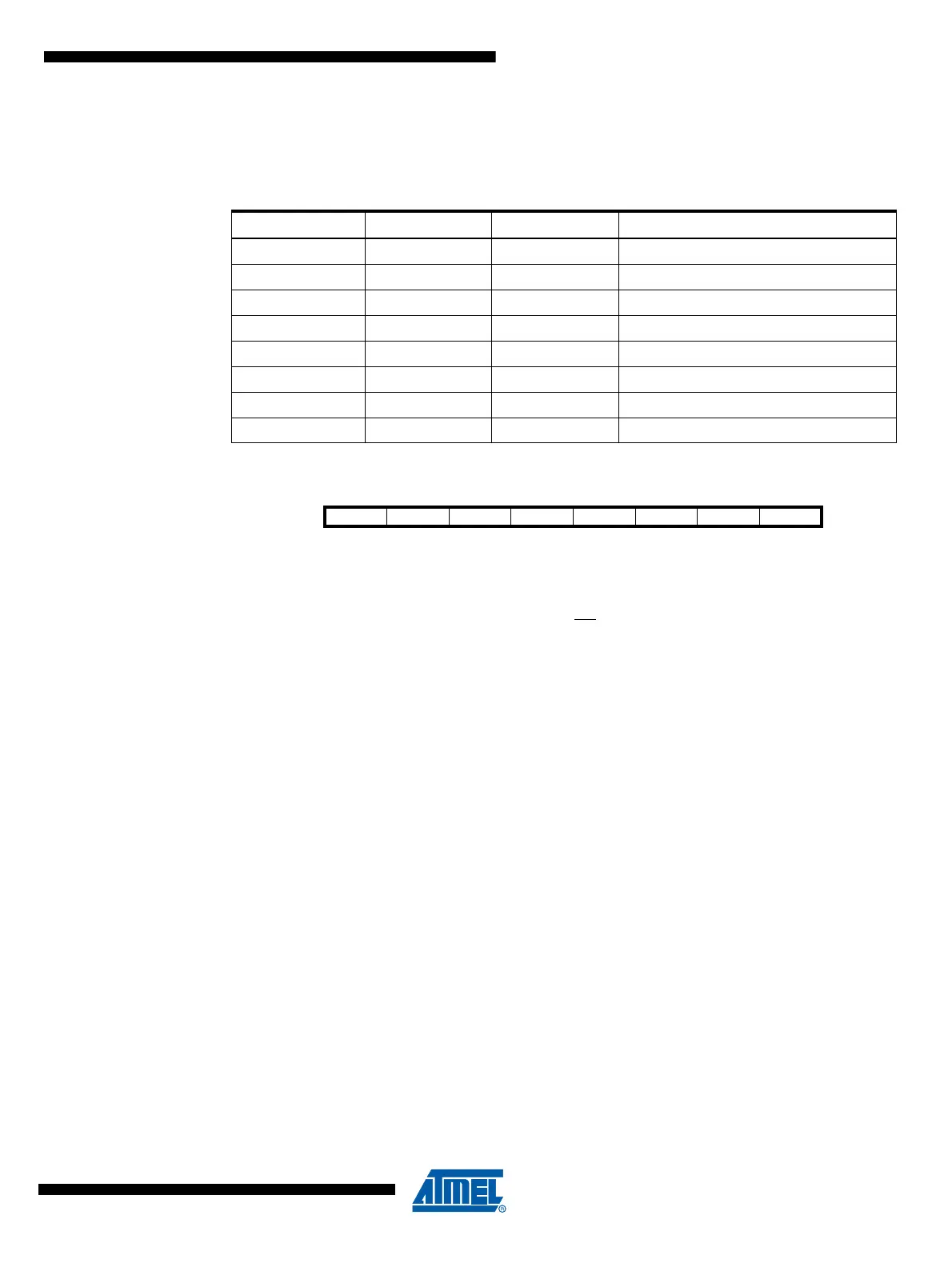
These two bits control the SCK rate of the device configured as a Master. SPR1 and SPR0 have
no effect on the Slave. The relationship between SCK and the clk
IO
frequency f
clkio
is shown in
the following table:
15.2.5 SPI Status Register – SPSR
Bit 7 – SPIF: SPI Interrupt Flag
When a serial transfer is complete, the SPIF flag is set. An interrupt is generated if SPIE in
SPCR is set and global interrupts are enabled. If SS
is an input and is driven low when the SPI is
in Master mode, this will also set the SPIF flag. SPIF is cleared by hardware when executing the
corresponding interrupt handling vector. Alternatively, the SPIF bit is cleared by first reading the
SPI Status Register with SPIF set, then accessing the SPI Data Register (SPDR).
Bit 6 – WCOL: Write COLlision Flag
The WCOL bit is set if the SPI Data Register (SPDR) is written during a data transfer. The
WCOL bit (and the SPIF bit) are cleared by first reading the SPI Status Register with WCOL set,
and then accessing the SPI Data Register.
Bit 5..1 – Res: Reserved Bits
These bits are reserved bits in the ATmega16/32/64/M1/C1 and will always read as zero.
Bit 0 – SPI2X: Double SPI Speed Bit
When this bit is written logic one the SPI speed (SCK Frequency) will be doubled when the SPI
is in Master mode (see Table 15-4). This means that the minimum SCK period will be two CPU
clock periods. When the SPI is configured as Slave, the SPI is only guaranteed to work at f
clkio
/4
or lower.
The SPI interface on the ATmega16/32/64/M1/C1 is also used for program memory and
EEPROM downloading or uploading. See Serial Programming Algorithm313 for serial program-
ming and verification.
Table 15-4. Relationship Between SCK and the Oscillator Frequency
SPI2X SPR1 SPR0 SCK Frequency
000
f
clkio
/4
001
f
clkio
/16
010f
clkio
/64
011f
clkio
/128
100
f
clkio
/2
101f
clkio
/8
110f
clkio
/32
111
f
clkio
/64
Bit 76543210
SPIF WCOL SPI2X SPSR
Read/Write R R R R R R R R/W
Initial Value 00000000

Table of Contents

Question and Answer IconNeed help?

Do you have a question about the Atmel ATmega32M1 and is the answer not in the manual?

Atmel ATmega32M1 Specifications

General IconGeneral
Architecture8-bit AVR
Flash Memory32 KB
SRAM2 KB
EEPROM1 KB
Clock Speed16 MHz
GPIO Pins32
I/O Pins32
ADC Channels8
ADC Resolution10-bit
UART1
USART1
SPI1
I2C1
PWM Channels6
CAN1
Operating Voltage2.7V - 5.5V
Operating Temperature-40°C to +85°C
Temperature Range-40°C to +85°C
Package44-TQFP, 44-QFN

Summary

Features

AVR CPU Core

Reset and Interrupt Handling

Explanation of interrupt sources, vectors, priority levels, and behavior during interrupt execution.

System Clock

System Clock Prescaler

Details on the CLKPR register for dividing the system clock to reduce power consumption and affect peripheral frequencies.

Power Management and Sleep Modes

8-bit Timer/Counter0 with PWM

Modes of Operation

Detailed explanation of Normal, CTC, and various PWM modes for Timer/Counter0 operation.

Controller Area Network - CAN

CAN Protocol

Explanation of the CAN protocol principles, standards, and message transmission priorities.

Error Management

Description of error detection mechanisms (message and bit level) and fault confinement states.

Analog to Digital Converter - ADC

Features

List of ADC capabilities including resolution, accuracy, conversion time, input channels, and reference voltages.

Starting a Conversion

Procedures for initiating ADC conversions, including single conversion and auto-triggering modes.

debugWIRE On-chip Debug System

Features

Overview of debugWIRE capabilities including program flow control, real-time operation, and symbolic debugging.

Boot Loader Support – Read-While-Write Self-Programming ATmega16/32/64/M1/C1

Self-Programming the Flash

Procedures and considerations for programming the Flash memory using the SPM instruction.

Memory Programming

Electrical Characteristics

Absolute Maximum Ratings*

Critical voltage, current, and temperature limits that must not be exceeded for device reliability.

Instruction Set Summary

Register Summary

Related product manuals