EasyManua.ls Logo

Atmel ATmega32M1 User Manual

Atmel ATmega32M1
367 pages
To Next Page IconTo Next Page
To Previous Page IconTo Previous Page
Page #22 background imageLoading...
Page #22 background image
22
7647H–AVR–03/12
Atmel ATmega16/32/64/M1/C1
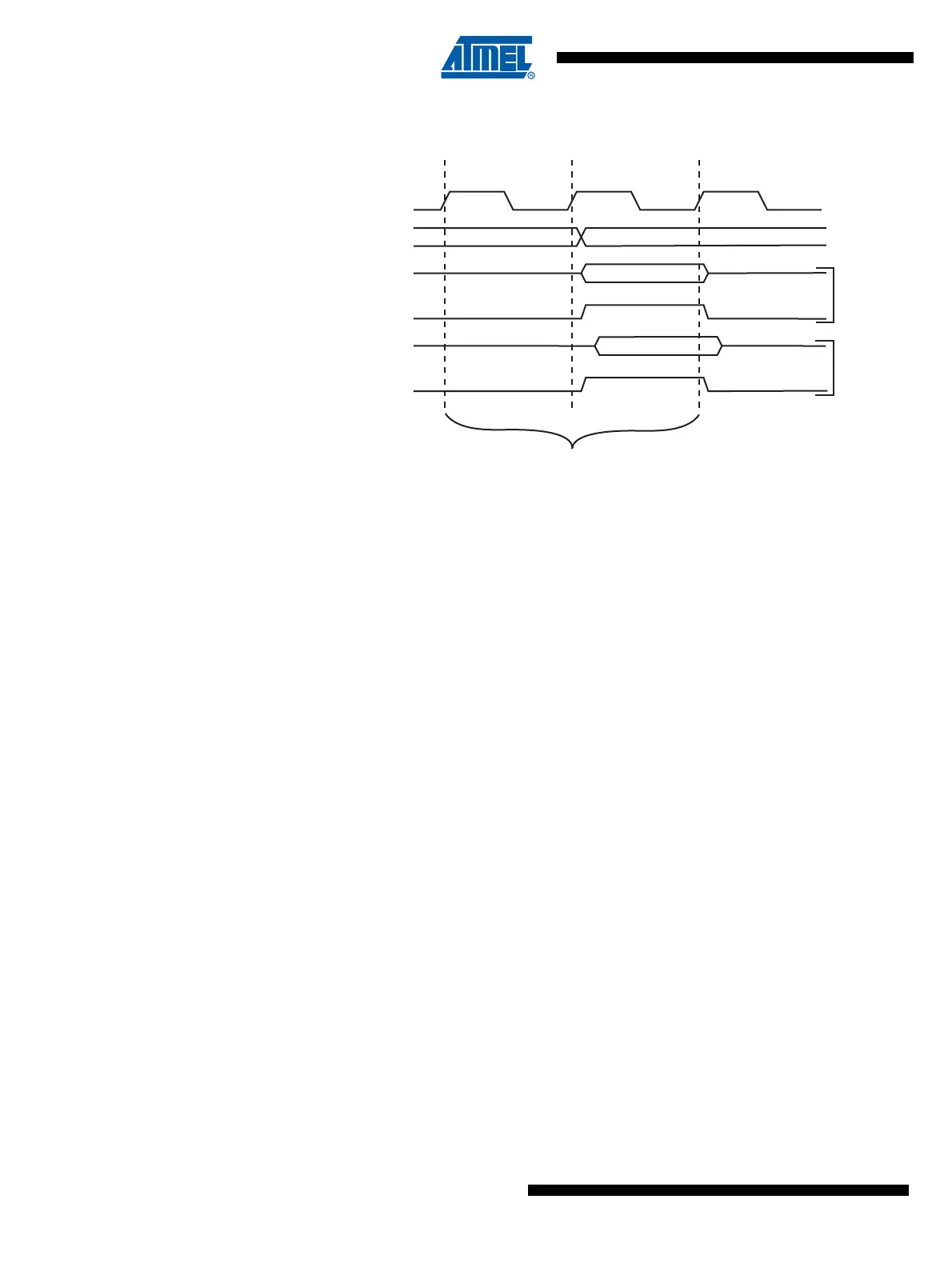
Figure 4-3. On-chip Data SRAM Access Cycles
4.3 EEPROM Data Memory
The ATmega16/32/64/M1/C1 contains 512/1024/2048 bytes of data EEPROM memory. It is
organized as a separate data space, in which single bytes can be read and written. The
EEPROM has an endurance of at least 100,000 write/erase cycles. The access between the
EEPROM and the CPU is described in the following, specifying the EEPROM Address Regis-
ters, the EEPROM Data Register, and the EEPROM Control Register.
For a detailed description of SPI and Parallel data downloading to the EEPROM, see “Serial
Downloading” on page 313 , and “Parallel Programming Parameters, Pin Mapping, and Com-
mands” on page 301 respectively.
4.3.1 EEPROM Read/Write Access
The EEPROM Access Registers are accessible in the I/O space.
The write access time for the EEPROM is given in Table 4-2. A self-timing function, however,
lets the user software detect when the next byte can be written. If the user code contains instruc-
tions that write the EEPROM, some precautions must be taken. In heavily filtered power
supplies, V
CC
is likely to rise or fall slowly on power-up/down. This causes the device for some
period of time to run at a voltage lower than specified as minimum for the clock frequency used.
See “Preventing EEPROM Corruption” on page 27.for details on how to avoid problems in these
situations.
In order to prevent unintentional EEPROM writes, a specific write procedure must be followed.
Refer to the description of the EEPROM Control Register for details on this.
When the EEPROM is read, the CPU is halted for four clock cycles before the next instruction is
executed. When the EEPROM is written, the CPU is halted for two clock cycles before the next
instruction is executed.
clk
WR
RD
Data
Data
Address
Address valid
T1 T2 T3
Compute Address
Read
Write
CPU
Memory Access Instruction
Next Instruction

Table of Contents

Question and Answer IconNeed help?

Do you have a question about the Atmel ATmega32M1 and is the answer not in the manual?

Atmel ATmega32M1 Specifications

General IconGeneral
Architecture8-bit AVR
Flash Memory32 KB
SRAM2 KB
EEPROM1 KB
Clock Speed16 MHz
GPIO Pins32
I/O Pins32
ADC Channels8
ADC Resolution10-bit
UART1
USART1
SPI1
I2C1
PWM Channels6
CAN1
Operating Voltage2.7V - 5.5V
Operating Temperature-40°C to +85°C
Temperature Range-40°C to +85°C
Package44-TQFP, 44-QFN

Summary

Features

AVR CPU Core

Reset and Interrupt Handling

Explanation of interrupt sources, vectors, priority levels, and behavior during interrupt execution.

System Clock

System Clock Prescaler

Details on the CLKPR register for dividing the system clock to reduce power consumption and affect peripheral frequencies.

Power Management and Sleep Modes

8-bit Timer/Counter0 with PWM

Modes of Operation

Detailed explanation of Normal, CTC, and various PWM modes for Timer/Counter0 operation.

Controller Area Network - CAN

CAN Protocol

Explanation of the CAN protocol principles, standards, and message transmission priorities.

Error Management

Description of error detection mechanisms (message and bit level) and fault confinement states.

Analog to Digital Converter - ADC

Features

List of ADC capabilities including resolution, accuracy, conversion time, input channels, and reference voltages.

Starting a Conversion

Procedures for initiating ADC conversions, including single conversion and auto-triggering modes.

debugWIRE On-chip Debug System

Features

Overview of debugWIRE capabilities including program flow control, real-time operation, and symbolic debugging.

Boot Loader Support – Read-While-Write Self-Programming ATmega16/32/64/M1/C1

Self-Programming the Flash

Procedures and considerations for programming the Flash memory using the SPM instruction.

Memory Programming

Electrical Characteristics

Absolute Maximum Ratings*

Critical voltage, current, and temperature limits that must not be exceeded for device reliability.

Instruction Set Summary

Register Summary

Related product manuals