224
7647H–AVR–03/12
Atmel ATmega16/32/64/M1/C1
– 01 = No CRC, no Time out (listen mode “off”),
– 10 = No Frame_Time_Out (listen mode “off” & CRC “on”),
– 11 = Listening mode (CRC “on” & Frame_Time_Out “on”).
b. UART mode (default = 00):
– 00 = 8-bit, no parity (listen mode “off”),
– 01 = 8-bit, even parity (listen mode “off”),
– 10 = 8-bit, odd parity (listen mode “off”),
– 11 = Listening mode, 8-bit, no parity.
• Bit 3 - LENA: Enable
– 0 = Disable (both LIN and UART modes),
– 1 = Enable (both LIN and UART modes).
• Bit 2:0 - LCMD[2..0]: Command and mode
The command is only available if LENA is set.
–000 = LIN Rx Header - LIN abort,
– 001 = LIN Tx Header,
– 010 = LIN Rx Response,
– 011 = LIN Tx Response,
– 100 = UART Rx & Tx Byte disable,
– 11x = UART Rx Byte enable,
– 1x1 = UART Tx Byte enable.
17.6.2 LIN Status and Interrupt Register - LINSIR
• Bits 7:5 - LIDST[2:0]: Identifier Status
– 0xx = no specific identifier,
– 100 = Identifier 60 (0x3C),
– 101 = Identifier 61 (0x3D),
– 110 = Identifier 62 (0x3E),
– 111 = Identifier 63 (0x3F).
• Bit 4 - LBUSY: Busy Signal
– 0 = Not busy,
– 1 = Busy (receiving or transmitting).
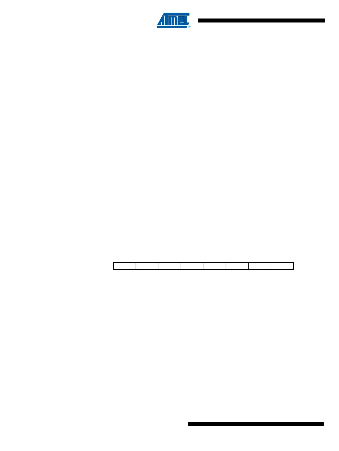
Bit 76543210
LIDST2 LIDST1 LIDST0 LBUSY LERR LIDOK LTXOK LRXOK
LINSIR
Read/WriteRRRRR/W
one
R/W
one
R/W
one
R/W
one
Initial Value00000000

 Loading...


