249
7647H–AVR–03/12
Atmel ATmega16/32/64/M1/C1
18.9.4 ADC Result Data Registers – ADCH and ADCL
When an ADC conversion is complete, the conversion results are stored in these two result data
registers.
When the ADCL register is read, the two ADC result data registers can’t be updated until the
ADCH register has also been read.
Consequently, in 10-bit configuration, the ADCL register must be read first before the ADCH.
Nevertheless, to work easily with only 8-bit precision, there is the possibility to left adjust the
result thanks to the ADLAR bit in the ADCSRA register. Like this, it is sufficient to only read
ADCH to have the conversion result.
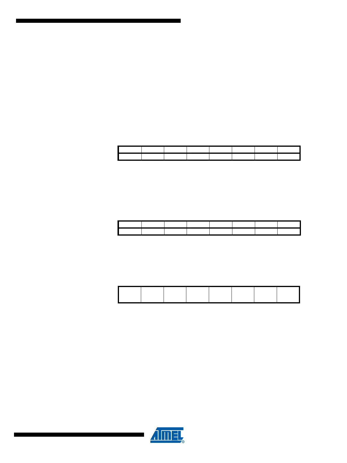
18.9.4.1 ADLAR = 0
18.9.4.2 ADLAR = 1
18.9.5 Digital Input Disable Register 0 – DIDR0
• Bit 7:0 – ADC7D..ADC0D, ACMPN0D, ACMPN1D, ACMPN2D, ACMPN3D, ACMP2D,
AMP2ND:
ADC7:0, ACMPN0, ACMPN1, ACMPN2, ACMPN3, ACMP2, AMP2N Digital Input Disable
When this bit is written logic one, the digital input buffer on the corresponding ADC pin is dis-
abled. The corresponding PIN Register bit will always read as zero when this bit is set. When an
analog signal is applied to the ADC7..0 pin and the digital input from this pin is not needed, this
bit should be written logic one to reduce power consumption in the digital input buffer.
Bit 76543210
- - - - - - ADC9 ADC8 ADCH
ADC7 ADC6 ADC5 ADC4 ADC3 ADC2 ADC1 ADC0 ADCL
Read/Write RRRRRRRR
RRRRRRRR
Initial Value00000000
00000000
Bit 76543210
ADC9 ADC8 ADC7 ADC6 ADC5 ADC4 ADC3 ADC2 ADCH
ADC1 ADC0 - - ----ADCL
Read/Write R R R R R R R R
RRRRRRRR
Initial Value00000000
00000000
Bit 76543210
ADC7D ADC6D
ACMPN1D
AMP2ND
ADC5D
ACMPN0D
ADC4D ADC3D
ACMPN2D
ADC2D
ACMP2D
ADC1D ADC0D
ACMPN3D
DIDR0
Read/Write R/W R/W R/W R/W R/W R/W R/W R/W
Initial Value 00000000