194
7647H–AVR–03/12
Atmel ATmega16/32/64/M1/C1
16.10.10 CAN Bit Timing Register 3 - CANBT3
• Bit 7– Reserved Bit
This bit is reserved for future use. For compatibility with future devices, it must be written to zero
when CANBT3 is written.
• Bit 6:4 – PHS22:0: Phase Segment 2
This phase is used to compensate for phase edge errors. This segment may be shortened by
the re-synchronization jump width. PHS2[2..0] shall be ≥1 and ≤PHS1[2..0] (c.f. Section 16.2.3
“CAN Bit Timing” on page 170 and Section 16.4.3 “Baud Rate” on page 177).
• Bit 3:1 – PHS12:0: Phase Segment 1
This phase is used to compensate for phase edge errors. This segment may be lengthened by
the re-synchronization jump width.
• Bit 0 – SMP: Sample Point(s)
This option allows to filter possible noise on TxCAN input pin.
– 0 - the sampling will occur once at the user configured sampling point - SP.
– 1 - with three-point sampling configuration the first sampling will occur two
Tclk
IO
clocks before the user configured sampling point - SP, again at one
Tclk
IO
clock
before SP and finally at SP. Then the bit level will be determined by a majority vote of
the three samples.
‘SMP=1’ configuration is not compatible with ‘BRP[5:0]=0’ because TQ =
Tclk
IO
.
If BRP = 0, SMP must be cleared.
16.10.11 CAN Timer Control Register - CANTCON
• Bit 7:0 – TPRSC7:0: CAN Timer Prescaler
Prescaler for the CAN timer upper counter range 0 to 255. It provides the clock to the CAN timer
if the CAN controller is enabled.
Tclk
CANTIM
= Tclk
IO
x 8 x (CANTCON [7:0] + 1)
Bit 76543210
- PHS22 PHS21 PHS20 PHS12 PHS11 PHS10 SMP CANBT3
Read/Write - R/W R/W R/W R/W R/W R/W R/W
Initial Value-0000000
Tphs2 = Tscl x (PHS2 [2:0] + 1)
Tphs1 = Tscl x (PHS1 [2:0] + 1)
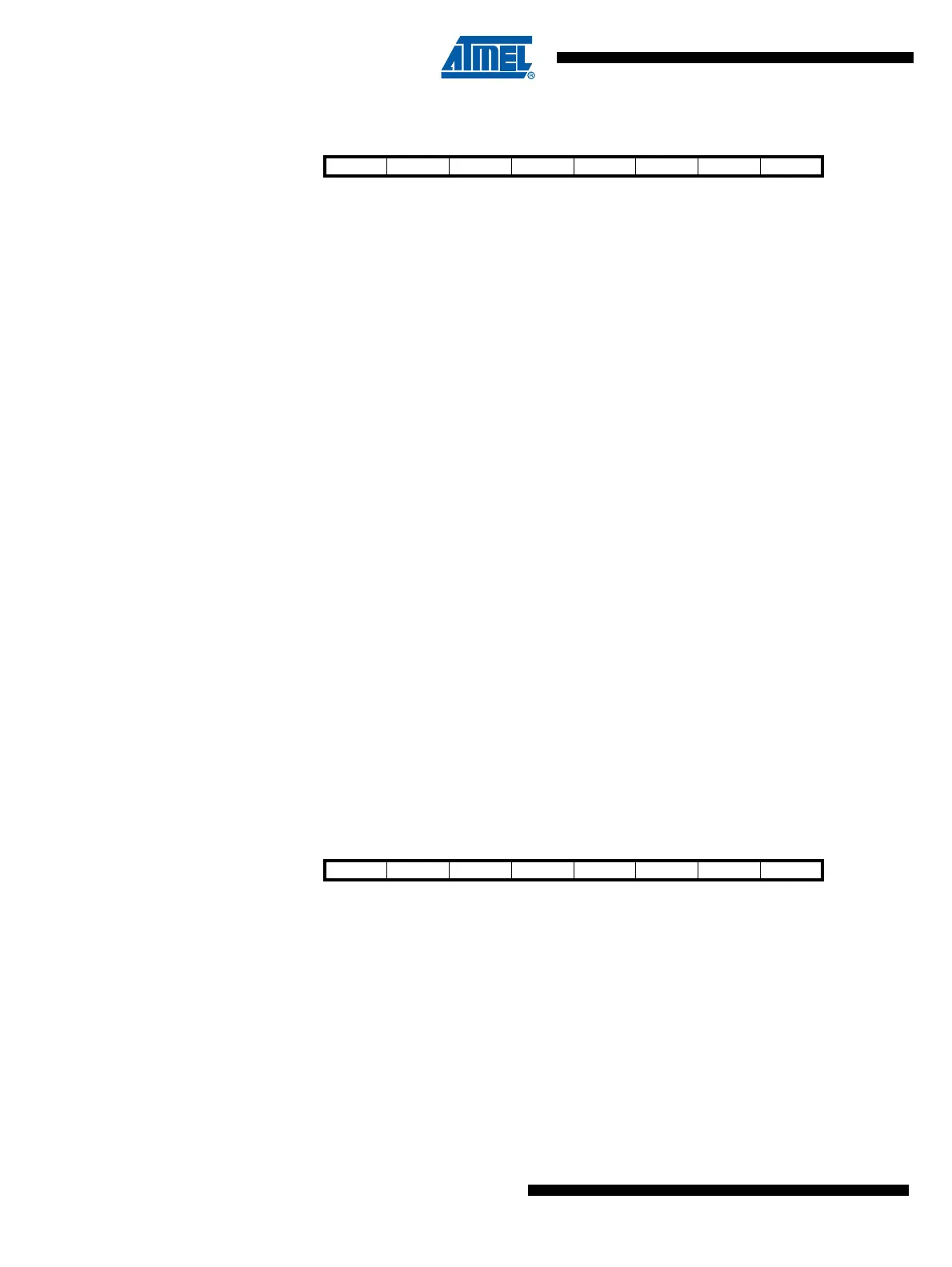
Bit 76543210
TPRSC7 TPRSC6 TPRSC5 TPRSC4 TPRSC3 TPRSC2 TRPSC1 TPRSC0 CANTCON
Read/Write R/W R/W R/W R/W R/W R/W R/W R/W
Initial Value00000000

 Loading...


