265
7647H–AVR–03/12
Atmel ATmega16/32/64/M1/C1
20.4.2 Analog Comparator 1Control Register – AC1CON
• Bit 7– AC1EN: Analog Comparator 1 Enable Bit
Set this bit to enable the analog comparator 1.
Clear this bit to disable the analog comparator 1.
• Bit 6– AC1IE: Analog Comparator 1 Interrupt Enable bit
Set this bit to enable the analog comparator 1 interrupt.
Clear this bit to disable the analog comparator 1 interrupt.
• Bit 5, 4– AC1IS1, AC1IS0: Analog Comparator 1 Interrupt Select bit
These 2 bits determine the sensitivity of the interrupt trigger.
The different setting are shown in Table 18-7.
• Bit 3– AC1ICE: Analog Comparator 1 Interrupt Capture Enable bit
Set this bit to enable the input capture of the Timer/Counter1 on the analog comparator event.
The comparator output is in this case directly connected to the input capture front-end logic,
making the comparator utilize the noise canceler and edge select features of the
Timer/Counter1 Input Capture interrupt. To make the comparator trigger the Timer/Counter1
Input Capture interrupt, the ICIE1 bit in the Timer Interrupt Mask Register (TIMSK1) must be set.
In case ICES1 bit (“Timer/Counter1 Control Register B – TCCR1B” on page 132) is set high, the
rising edge of AC1O is the capture/trigger event of the Timer/Counter1, in case ICES1 is set to
zero, it is the falling edge which is taken into account.
Table 20-2. Analog Comparator 0 negative input selection
AC0M2 AC0M1 AC0M0 Description
000“Vref”/6.40
001“Vref”/3.20
010“Vref”/2.13
011“Vref”/1.60
100Bandgap (1.1V)
101DAC result
110Analog Comparator Negative Input (ACMPM pin)
111Reserved
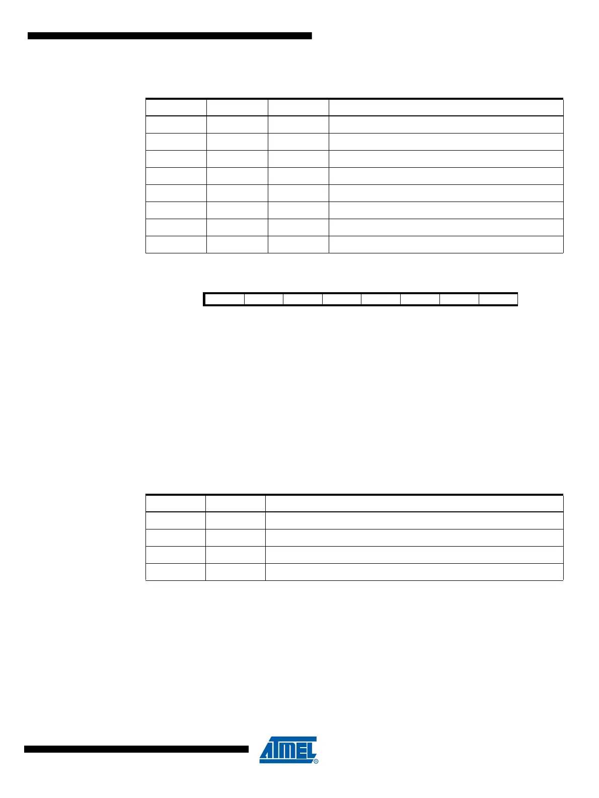
Bit 76543210
AC1EN AC1IE AC1IS1 AC1IS0 AC1ICE AC1M2 AC1M1 AC1M0 AC1CON
Read/Write R/W R/W R/W R/W R/W R/W R/W R/W
Initial Value 00000000
Table 20-3. Interrupt sensitivity selection
AC1IS1 AC1IS0 Description
0 0 Comparator Interrupt on output toggle
01Reserved
1 0 Comparator interrupt on output falling edge
1 1 Comparator interrupt on output rising edge