PCB design and manufacturing Recommended solder reflow cycle
XBee®/XBee-PRO SX RF Module User Guide
204
the module. All of the grounds on the jack and the module are connected to the ground planes directly
or through closely placed vias. Space any ground fill on the top layer at least twice the distance d (in
this case, at least 0.050 in) from the microstrip to minimize their interaction.
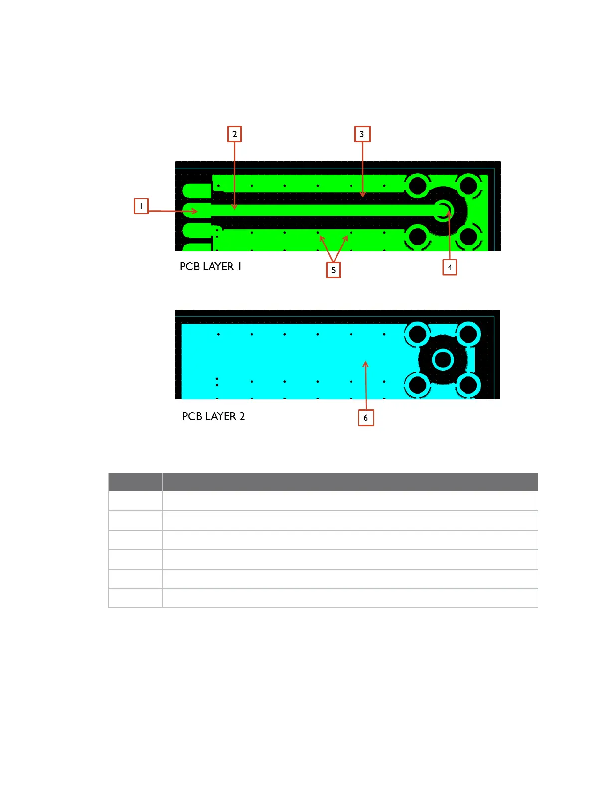
Number Description
1
XBee pin 36
2 50 Ω microstrip trace
3 Back off ground fill at least twice the distance between layers 1 and 2
4 RF connector
5 Stitch vias near the edges of the ground plane
6 Pour a solid ground plane under the RF trace on the reference layer
Implementing these design suggestions helps ensure that the RFpad device performs to
specifications.
Recommended solder reflow cycle
The following table provides the recommended solder reflow cycle. The table shows the temperature
setting and the time to reach the temperature; it does not show the cooling cycle.