GE Energy
D20/D200
Installation and Operations Guide
General 994-0078-2.00-7
Full
43
Connections and Configuration, continued
D20ME Jumpering, continued
D20ME
Jumper
Options
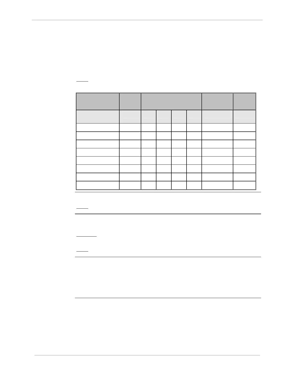
The following tables su
mmarize the jumper settings for the D20ME main processor
board.
Note:
Single Node D20 is the factory default configuration.
Board Function JP1
Master /
Slave
JP2
VME Address Bits
4 3 2 1
JP3-1
RTC -
SERCLOCK
JP3-2
RTC -
BTRC
Single Node D20
(see note above)
OUT IN IN IN IN OUT IN
Lead Node of D200 OUT IN IN IN OUT IN IN
Non-lead Node #2 IN IN IN OUT IN IN OUT
Non-lead Node #3 IN IN IN OUT OUT IN OUT
Non-lead Node #4 IN IN OUT IN IN IN OUT
Non-lead Node #5 IN IN OUT IN OUT IN OUT
Non-lead Node #6 IN IN OUT OUT IN IN OUT
Non-lead Node #7 IN IN OUT OUT OUT IN OUT
Non-lead Node #8 IN OUT IN IN IN IN OUT
JP1 - VME
Control
This jumper sets the Master or Slave role of the board on the VME bus.
Note:
Single-node (D20) systems are always set to Master
JP2 - VME
Address
JP2 is a group of four jumpers that set the VME bus address of the board. The
address should reflect the board location in a D200 CCU chassis.
Example:
The board with address 1 will be the lead node, with nodes 2 through 8
positioned to the right of the lead node.
Note:
Single-node D20s are set to address 0 (all jumpers IN)
JP3-1 and
JP3-2
RTC Options
These two jumpers determine the Real Time Clock (RTC) source for each D20ME
board in a CCU.
• Single-node D20s and the first, or Lead, node of a D200 will use their internal
clock.
• Non-lead nodes of a D200 must synchronize their clocks to node 1’s clock.