Appendix HIMax System
HI 801 001 E Rev. 4.01 Page 118 of 122
Index of Figures
Figure 1: System Overview 16
Figure 2: Base Plate Structure 17
Figure 3: Arrangement of Racks on the System Bus 21
Figure 4: System Bus with Network Structure 23
Figure 5: Maximum distance for latency default value 26
Figure 6: Maximum distance between processor modules with latency default value 27
Figure 7: Connection of Two Base Plates through a Fiber Optic Cable 28
Figure 8: Example for Calculating the System Bus Latency 30
Figure 9: Transient Interference 39
Figure 10: Interference Triggers Safe Reaction 40
Figure 11: Effective Direction Associated with Noise Blanking and Output Noise Blanking 41
Figure 12: CPU Cycle Sequence with Multitasking 69
Figure 13: Multitasking Mode 1 72
Figure 14: Multitasking Mode 2 73
Figure 15: Multitasking Mode 3 74
Figure 16: Wiring 1 - Single Connector Board with Screw Terminals 93
Figure 17: Wiring 2 - Redundant Connector Board with Screw Terminals 94
Figure 18: Wiring 3 - Single Connector Board with System Cable 95
Figure 19: Wiring 4 - Redundant Connector Board with System Cable 96
Figure 20: Earthing Connections in the Control Cabinet 98
Figure 21: Earthing and Shielding the 19" Control Cabinet 99
Figure 22: Earth Connections for Base Plate 100
Figure 23: Earth Terminals of Various Control Cabinets 101
Figure 24: Inserting the Connector Board 103
Figure 25: Securing the Connector Board with Captive Screws 104
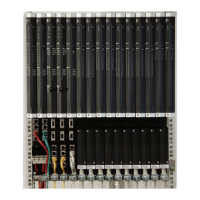
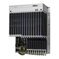
Figure 26: Small HIMax System: One Base Plate, Two Processor Modules 115
Figure 27: Minimum System without Redundancy 115
Figure 28: HIMax System with Distributed Redundancy 116