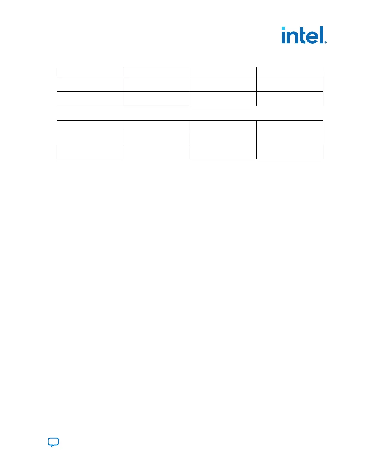
Table 39. Arria 10 I
2
C Signals
Schematic Signal Name Pin Number I/O Standard Description
DISP_I2C_SCL AW33 1.8 V Arria 10 I
2
C serial clock to
level shifter.
DISP_I2C_SDA AY34 1.8 V Arria 10 I
2
C serial data to
level shifter.
Table 40. Arria 10 I
2
C Level Shifter to LCD Signals
Schematic Signal Name LCD Pin Number I/O Standard Description
I2C_SCL_DISP 7 5.0 V LCD I
2
C serial clock from
Arria 10 FPGA level shifter.
I2C_SDA_DISP 8 5.0 V LCD I
2
C serial data from
Arria 10 FPGA level shifter.
6. Board Components
683526 | 2023.07.12
Send Feedback
Intel
®
Arria
®
10 FPGA Development Kit User Guide
101

 Loading...


