6.7.3. HiLo External Memory Interface
This section describes the Arria 10 GX FPGA development board’s external memory
interface support and also their signal names, types, and connectivity relative to the
Arria 10 GX FPGA.
The HiLo connector supports plugins the following memory interfaces:
• DDR3 x72 (included in the kit)
• DDR4 x72 (included in the kit)
• RLDRAM3 x36 (included in the kit)
• QDR IV x36 (not included. Contact your local Altera sales representative for
ordering and availability)
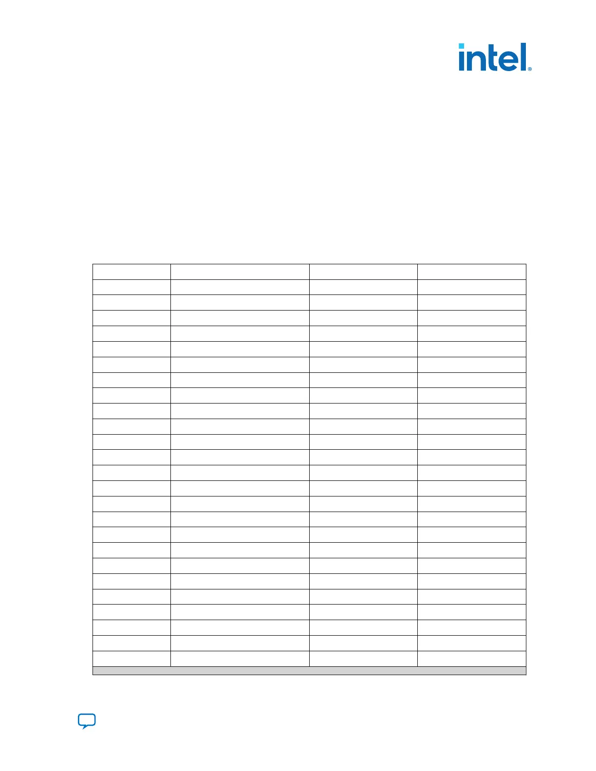
Table 32. HiLo EMI Pin Assignments, Schematic Signal Names
Board Reference Schematic Signal Name FPGA Pin Number I/O Standard
F1 MEM_ADDR_CMD0 M32 1.5 V
H1 MEM_ADDR_CMD1 L32 1.5 V
F2 MEM_ADDR_CMD2 N34 1.5 V
G2 MEM_ADDR_CMD3 M35 1.5 V
H2 MEM_ADDR_CMD4 L34 1.5 V
J2 MEM_ADDR_CMD5 K34 1.5 V
K2 MEM_ADDR_CMD6 M33 1.5 V
G3 MEM_ADDR_CMD7 L33 1.5V
J3 MEM_ADDR_CMD8 J33 1.5 V
L3 MEM_ADDR_CMD9 J32 1.5 V
E4 MEM_ADDR_CMD10 H31 1.5 V
F4 MEM_ADDR_CMD11 J31 1.5 V
G4 MEM_ADDR_CMD12 H34 1.5 V
H4 MEM_ADDR_CMD13 H33 1.5 V
J4 MEM_ADDR_CMD14 G32 1.5 V
K4 MEM_ADDR_CMD15 E32 1.5 V
M1 MEM_ADDR_CMD16 F33 1.5 V
M2 MEM_ADDR_CMD17 G35 1.5 V
N2 MEM_ADDR_CMD18 H35 1.5 V
L4 MEM_ADDR_CMD19 G33 1.5 V
P5 MEM_ADDR_CMD20 U33 1.5 V
M5 MEM_ADDR_CMD21 T33 1.5 V
P1 MEM_ADDR_CMD22 R34 1.5 V
R4 MEM_ADDR_CMD23 P34 1.5 V
M4 MEM_ADDR_CMD24 N33 1.5 V
continued...
6. Board Components
683526 | 2023.07.12
Send Feedback
Intel
®
Arria
®
10 FPGA Development Kit User Guide
81