6.7.7. I
2
C
I
2
C supports communication between integrated circuits on a board. It is a simple
two-wire bus that consists of a serial data line (SDA) and a serial clock (SCL). The
MAX V and Arria 10 devices use the I
2
C for reading and writing to the character LCD.
You can use the Arria 10 or MAX V as the I
2
C host to access the PLLs and clocks.
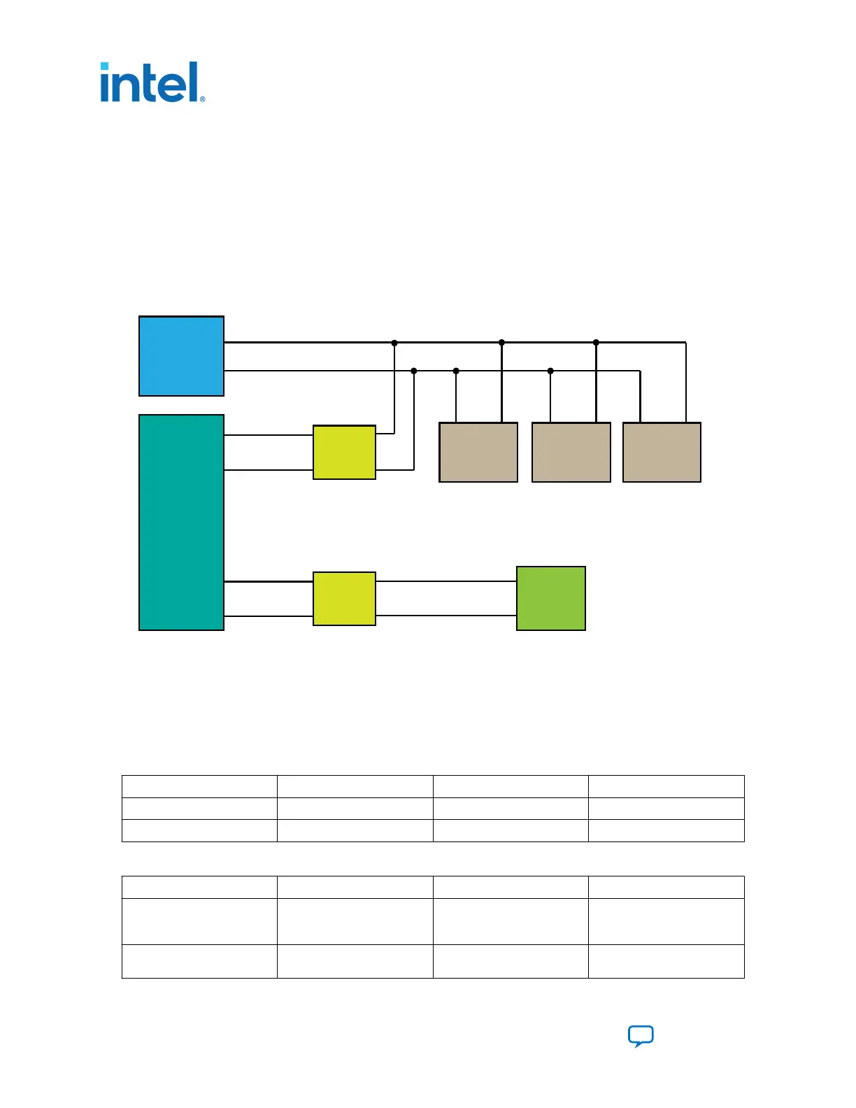
Figure 34. I
2
C Block Diagram
MAX V
Arria10
LCD
i2c_SCL_DISP
i2c_SDA_DISP
CLOCK_I2C_SDA
CLOCK_I2C_SCL
Level
Shift
Level
Shift
CLOCK_SCL
CLOCK_SDA
DISP_I2C_SCL
DISP_I2C_SDA
Si570 Si5338 Si5338
1.8V
1.8V
5.0V
2.5V
Table 37. MAX V I
2
C Signals
Schematic Signal Name Pin Number I/O Standard Description
CLOCK_I2C_SCL C12 2.5 V I
2
C serial clock from MAX V.
CLOCK_I2C_SDA C10 2.5 V I
2
C serial data from MAX V.
Table 38. MAV I
2
C Level Shifter Signals to Arria 10 FPGA
Schematic Signal Name Arria 10 Pin Number I/O Standard Description
CLOCK_SCL AN30 1.8 V Arria 10 FPGA I
2
C serial
clock from MAX V level
shifter.
CLOCK_SDA AV33 1.8 V Arria 10 FPGA I
2
C serial data
from MAX V level shifter.
6. Board Components
683526 | 2023.07.12
Intel
®
Arria
®
10 FPGA Development Kit User Guide
Send Feedback
100