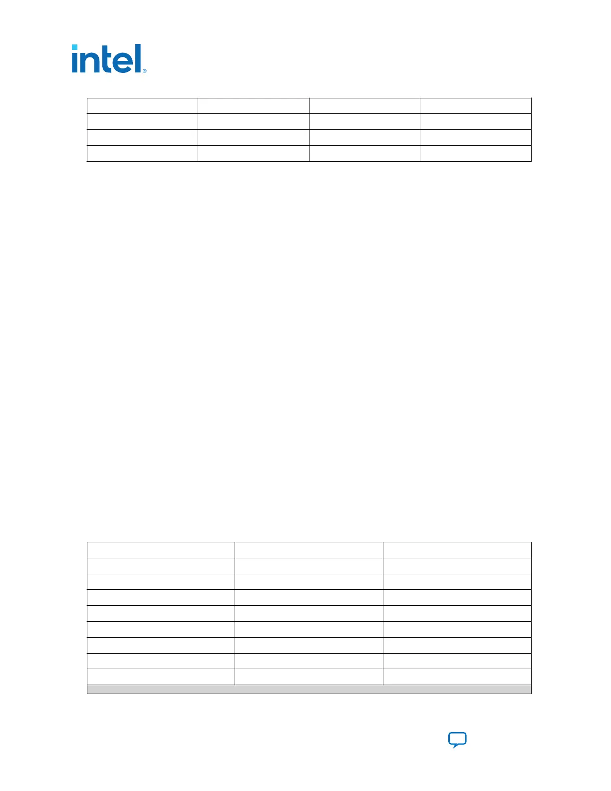
Schematic Signal Name Pin Number I/O Standard Description
ED8101_ALERT B8 2.5 V ED8101 Alert signal
ED8101_SCL A8 2.5 V ED8101 I2C clock signal
ED8101_SDA A9 2.5 V ED8101 I2C data signal
6.3. FPGA Configuration
6.3.1. Configuring the FPGA Using Programmer
You can use the Quartus Programmer to configure the FPGA with your SRAM Object
File (.sof).
Ensure the following:
• The Quartus Programmer and the USB-Blaster II driver are installed on the host
computer.
• The micro-USB cable is connected to the FPGA development board.
• Power to the board is on, and no other applications that use the JTAG chain are
running.
1. Start the Quartus Programmer.
2. Click Auto Detect to display the devices in the JTAG chain.
3.
Click Change File and select the path to the desired .sof.
4. Turn on the Program/Configure option for the added file.
5. Click Start to download the selected file to the FPGA. Configuration is complete
when the progress bar reaches 100%.
Using the Quartus Programmer to configure a device on the board causes other JTAG-
based applications such as the Board Test System and the Power Monitor to lose their
connection to the board. Restart those applications after configuration is complete.
6.4. Status Elements
The Arria 10 GX FPGA development board includes status LEDs.
Table 17. Board-Specific LEDs
Board Reference Schematic Signal Name I/O Standard
D16 MAX_ERROR 2.5 V
D15 MAX_LOAD 2.5 V
D17 MAX_CONF_DONE 2.5 V
D1 FMCA_TX_LED 1.8 V
D2 FMCA_RX_LED 1.8 V
D12 PGM_LED0 2.5 V
D13 PGM_LED1 2.5 V
D14 PGM_LED2 2.5 V
continued...
6. Board Components
683526 | 2023.07.12
Intel
®
Arria
®
10 FPGA Development Kit User Guide
Send Feedback
66