6.5.5. DisplayPort
The Arria 10 GX FPGA development board includes a DisplayPort connector.
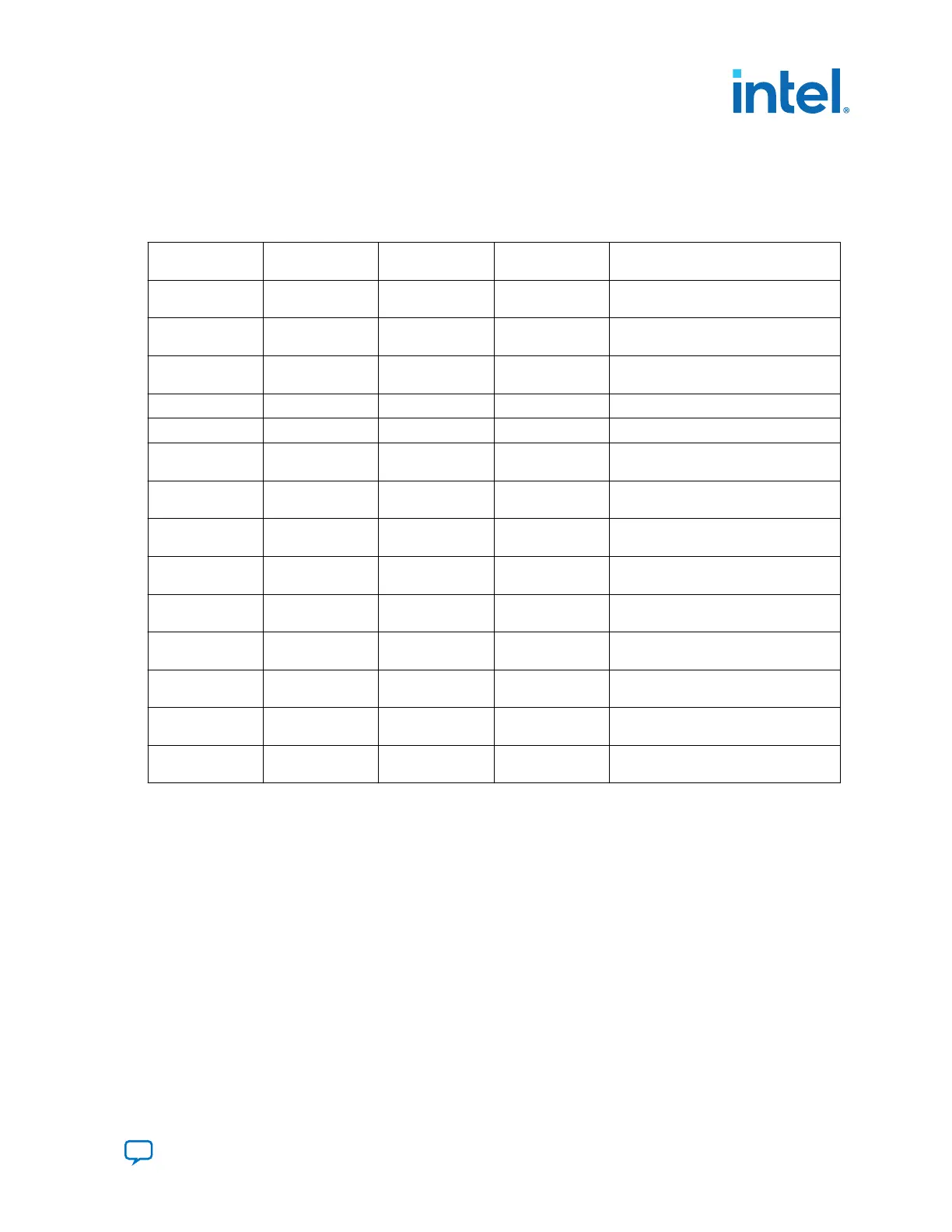
Table 22. DisplayPort Schematic Signal Names and Functions
Board Reference Schematic Signal
Name
FPGA Pin Number I/O Standard Description
13 DP_3P3V_CONFIG
1
AK31 1.8 V —
14 DP_3P3V_CONFIG
2
AK32 1.8 V —
18 DP_3P3V_HOT_PL
UG
AM30 1.8 V Hot plug detect
17 DP_AUX_CN AM35 LVDS Auxiliary channel (negative)
15 DP_AUX_CP AN34 LVDS Auxiliary channel (positive)
3 DP_ML_LANE_CN
0
AP43 High Speed
Differential I/O
Lane 0 (negative)
6 DP_ML_LANE_CN
1
AM43 High Speed
Differential I/O
Lane 1 (negative)
9 DP_ML_LANE_CN
2
AH43 High Speed
Differential I/O
Lane 2 (negative)
12 DP_ML_LANE_CN
3
AF43 High Speed
Differential I/O
Lane 3 (negative)
1 DP_ML_LANE_CP0 AP44 High Speed
Differential I/O
Lane 0 (positive)
4 DP_ML_LANE_CP1 AM44 High Speed
Differential I/O
Lane 1 (positive)
7 DP_ML_LANE_CP2 AH44 High Speed
Differential I/O
Lane 2 (positive)
10 DP_ML_LANE_CP3 AF44 High Speed
Differential I/O
Lane 3 (positive)
19 DP_RTN AL33 High Speed
Differential I/O
Return for power
6. Board Components
683526 | 2023.07.12
Send Feedback
Intel
®
Arria
®
10 FPGA Development Kit User Guide
71