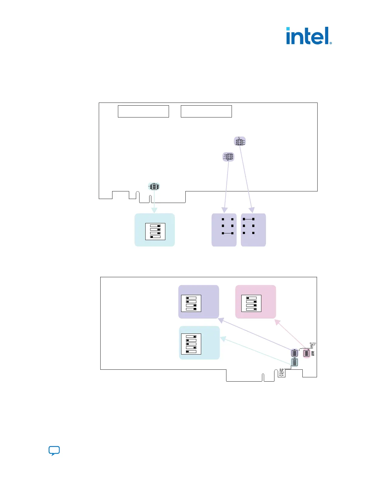
3.3. Default Switch and Resistor Settings
This topic shows you how to restore the default factory settings and explains their
functions.
Figure 7. Default Switch and Resistor Settings on the Top
FMCBFMCA
SW3
PRSNTn
ON
4 3 2 1
X1
X4
X8
FMCB
VCCIO
1.8V
1.5V
1.35V
FMCA
Note:
No shunt = 1.2V
1.35V
1.5V
1.8V
R1084
R1085
R1086
R1081
R1082
R1083
Figure 8. Default Switch Settings on the Bottom
SW5
ON
1 2 3 4
MSEL0
MSEL1
MSEL2
VIDEN
SW4
CLK_SEL
CLK_EN
Si516_FS
FACTORY
RZQ_B2K
ON
1
1 0 1 0
2 3 4
ARRIA 10
MAX V
FMCA
FMCB
SW6
ON
1 2 3 4 5
1. Set DIP switch bank (SW3) to match the following table.
3. Development Board Setup
683526 | 2023.07.12
Send Feedback
Intel
®
Arria
®
10 FPGA Development Kit User Guide
15

 Loading...


