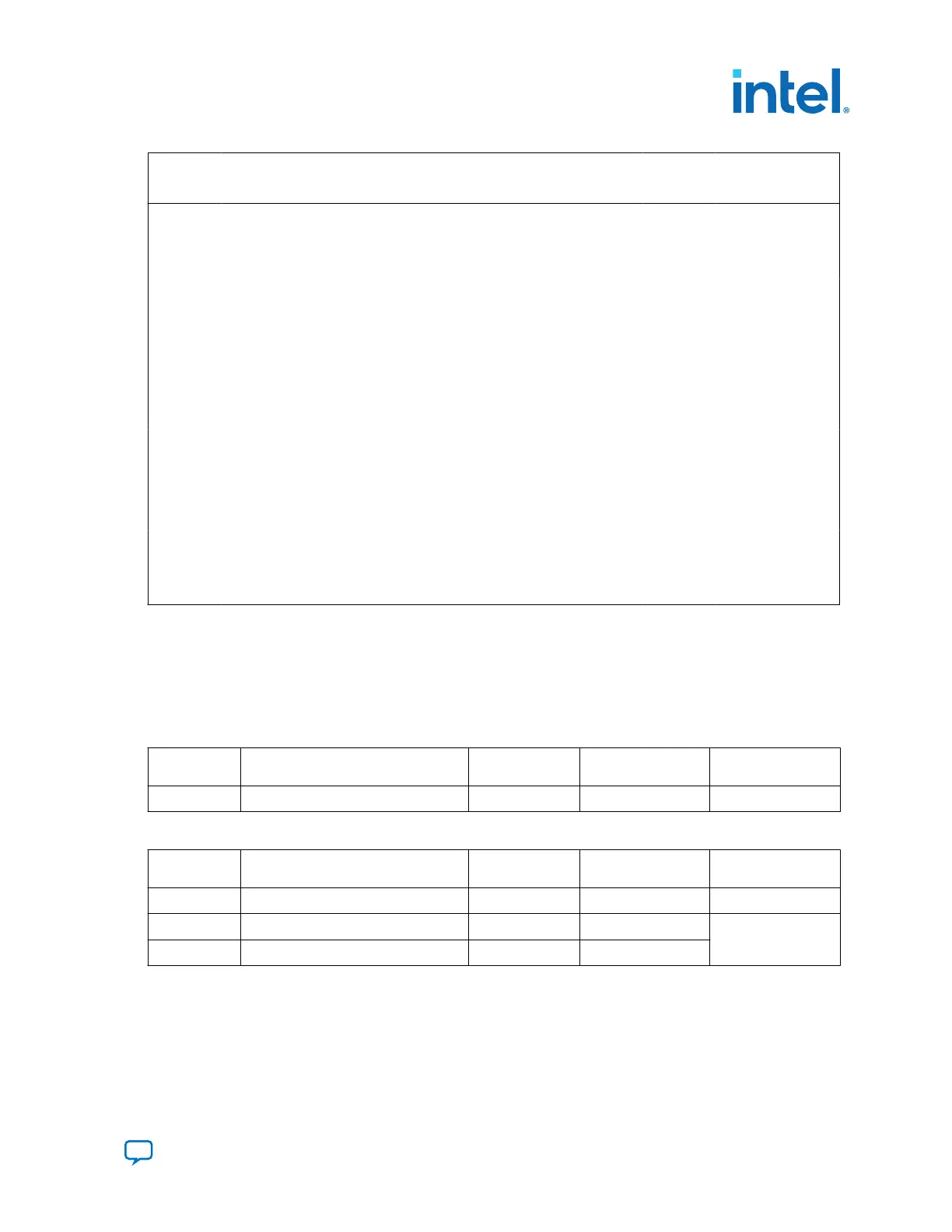
Source Schematic Signal Name Frequency I/O Standard Arria 10
FPGA Pin
Number
Application
REFCLK_QSFP_N
1.8 V LVDS R38
REFCLK_SFP_P
644.53125 MHz 1.8 V LVDS AA37 SFP reference
clocks
REFCLK_SFP_N
1.8 V LVDS AA38
REFCLK_DP_P
270 MHz 1.8 V LVDS AC37 Display port (DP)
reference clocks
REFCLK_DP_N
1.8 V LVDS AC38
X1
REFCLK_SDI_P
148.35 MHz 1.8 V LVDS L37 SDI reference
clocks
REFCLK_SDI_N
1.8 V LVDS L38
X2
CLK_125_P
125 MHz 1.8 V LVDS BD24 125 MHz reference
clocks for Arria 10
FPGA
CLK_125_N
1.8 V LVDS BC24
X3
100M_OSC_P
100 MHz LVDS AR36,
F23,
AG37, AC8
Programmable
Oscillator default
100MHz
100M_OSC_N
LVDS AR37,
G23,
AG38, AC7
U53
MV_CLK_50
50 MHz 1.8 V - MAX V System
Controller clock
CLK_50
1.8 V AU33 Arria 10 FPGA
reference clock
6.6.2. Off-Board Clock I/O
The development board has input and output clocks which can be driven onto the
board. The output clocks can be programmed to different levels and I/O standards
according to the FPGA device’s specification.
Table 28. Off-Board Clock Inputs
Source Schematic Signal Name I/O Standard Arria 10 FPGA Pin
Number
Description
J6
CLKIN_SMA
2.5 V - SMA clock input
Table 29. Off-Board Clock Outputs
Source Schematic Signal Name I/O Standard Arria 10 FPGA Pin
Number
Description
J7
SMA_CLK_OUT
1.8 V E24 SMA clock output
J16
SMA_TX_P
1.8 V C42 SMA transfer clocks
J15
SMA_TX_N
1.8 V C41
6. Board Components
683526 | 2023.07.12
Send Feedback
Intel
®
Arria
®
10 FPGA Development Kit User Guide
75