6.7. Components and Interfaces
This section describes the development board's communication ports and interface
cards relative to the Arria 10 GX FPGA device.
6.7.1. PCI Express
The Arria 10 GX FPGA development board is designed to fit entirely into a PC
motherboard with a ×8 PCI Express slot that can accommodate a full height long form
factor add-in card. This interface uses the Arria 10 GX FPGA's PCI Express hard IP
block, saving logic resources for the user logic application. The PCI express edge
connector has a presence detect feature to allow the motherboard to determine if a
card is installed.
The PCI Express interface supports auto-negotiating channel width from ×1 to ×4 to
×8 by using Altera's PCIe MegaCore IP. You can also configure this board to a ×1, ×4,
or ×8 interface through a DIP switch that connects the PRSNTn pins for each bus
width.
The PCI Express edge connector has a connection speed of 2.5 Gbps/lane for a
maximum of 20 Gbps full-duplex (Gen1), 5.0 Gbps/lane for a maximum of 40 Gbps
full-duplex (Gen2), or 8.0 Gbps/lane for a maximum of 64 Gbps full-duplex (Gen3).
The power for the board can be sourced entirely from the PC host when installed into
a PC motherboard with the PC's 2x4 ATX auxiliary power connected to the 12V ATX
input (J4) of the Arria 10 development board. Although the board can also be powered
by a laptop power supply for use on a lab bench, Altera recommends that you do not
power up from both supplies at the same time. Ideal diode power sharing devices
have been designed into this board to prevent damages or back-current from one
supply to the other.
The PCIE_REFCLK_P signal is a 100 MHz differential input that is driven from the PC
motherboard on to this board through the edge connector. This signal connects
directly to a Arria 10 GX FPGA REFCLK input pin pair using DC coupling. This clock is
terminated on the motherboard and therefore, no on-board termination is required.
This clock can have spread-spectrum properties that change its period between 9.847
ps to 10.203 ps. The I/O standard is High-Speed Current Steering Logic (HCSL). The
JTAG and SMB are optional signals in the PCI Express specification. Therefore, the
JTAG signal loopback from PCI Express TDI to PCI Express TDO and are not used on
this board. The SMB signals are wired to the Arria 10 GX FPGA but are not required for
normal operation.
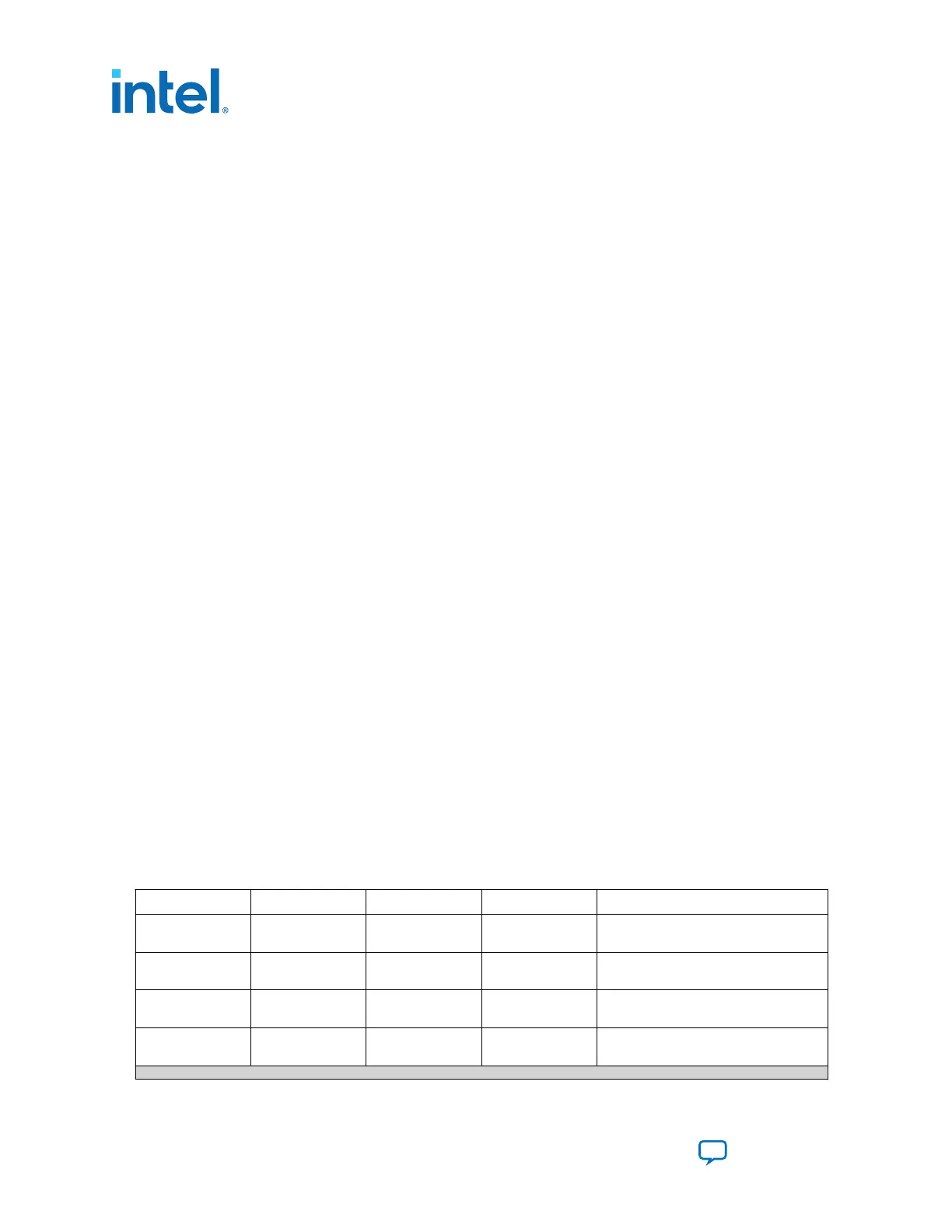
Table 30. PCI Express Pin Assignments, Schematic Signal Names, and Functions
Receive bus Receive bus FPGA Pin Number I/O Standard Description
A11 PCIE_EDGE_PERS
TN
BC30 1.8 V Reset
A14 PCIE_EDGE_REFC
LK_N
AL38 LVDS Motherboard reference clock
A13 PCIE_EDGE_REFC
LK_P
AL37 LVDS Motherboard reference clock
B5 PCIE_EDGE_SMBC
LK
BD29 1.8 V SMB clock
continued...
6. Board Components
683526 | 2023.07.12
Intel
®
Arria
®
10 FPGA Development Kit User Guide
Send Feedback
76