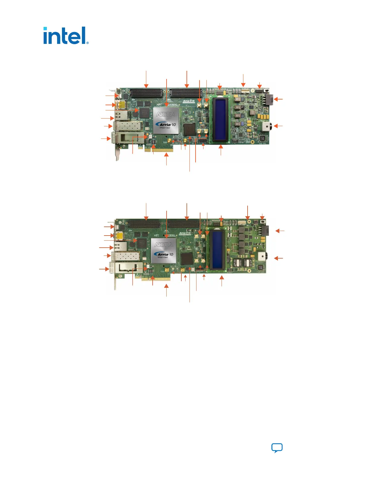
Figure 2. Overview of the Development Board Features (ES Edition)
FMCA (J1)
FMCB (J2)
Arria 10
FPGA (U28)
Clock In/Out
SMA (J6, J7)
User Dipswitch
(SW2)
Power Switch
(SW1)
PCIe ATX
Connector
(J4)
DC Input Jack
(J13)
JTAG Header
(J17)
Character LCD
(B2)
Transceiver TX
(J15, J16)
HiLo Connector
(J14)
SDI Video Port
(J20, J21)
PCI Express
Edge Connector
(J22)
PCIe Dipswitch
(SW3)
Fan Power
Header (J19)
On-Board
USB-Blaster II (J3)
DisplayPort
Connector (J5)
MAX V CPLD (U16)
Gbps Ethernet
Port (J9)
QSFP
Interface (J18)
LTPowerPlay interface
Connector (J24)
SFP+ Interface (J12)
Figure 3. Overview of the Development Board Features
FMCA (J1)
FMCB (J2)
Arria 10
FPGA (U28)
Clock In/Out
SMA (J6, J7)
User Dipswitch
(SW2)
Power Switch
(SW1)
PCIe ATX
Connector
(J4)
DC Input Jack
(J13)
JTAG Header
(J17)
Character LCD
(B2)
Transceiver TX
(J15, J16)
HiLo Connector
(J14)
SDI Video Port
(J20, J21)
PCI Express
Edge Connector
(J22)
PCIe Dipswitch
(SW3)
Fan Power
Header (J19)
On-Board
USB-Blaster II (J3)
DisplayPort
Connector (J5)
MAX V CPLD (U16)
Gbps Ethernet
Port (J9)
QSFP
Interface (J18)
LTPowerPlay interface
Connector (J24)
SFP+ Interface (J12)
Related Information
Board Components on page 55
For details on the board components.
1.2. Recommended Operating Conditions
• Recommended ambient operating temperature range: 0C to 45C
• Maximum ICC load current: 80A
• Maximum ICC load transient percentage: 35%
• FPGA maximum power supported by the supplied heatsink/fan: 100W
1. Intel
®
Arria
®
10 FPGA Development Kit Overview
683526 | 2023.07.12
Intel
®
Arria
®
10 FPGA Development Kit User Guide
Send Feedback
6
 Loading...


