6.7.4. FMC
The Arria 10 GX FPGA development board includes a high pin count (HPC) FPGA
mezzanine card (FMC) connector that functions with a quadrature amplitude
modulation (QAM) digital-to-analog converter (DAC) FMC module or daughtercard.
This pin-out satisfies a QAM DAC that requires 58 LVDS data output pairs, one LVDS
input clock pair, and three low-voltage differential signaling (LVDS) control pairs from
the FPGA device. These pins also have the option to be used as single-ended I/O pins.
The VCCIO supply for the FMC A and FMC B banks provide a variable voltage of 1.2V -
1.8V. The default voltage value is 1.8V.
However, for device safety concerns, a jumper is available for you to connect this bank
to the same VCCIO used for the FMC A banks. This allows the VCCIO pins on the FPGA
to be tied to a known power. The VCCIO pins also allows you the option to perform a
manual check for the module’s input voltage before connecting to the FPGA. This is to
ensure that the module does not exceed the power supply maximum voltage rating.
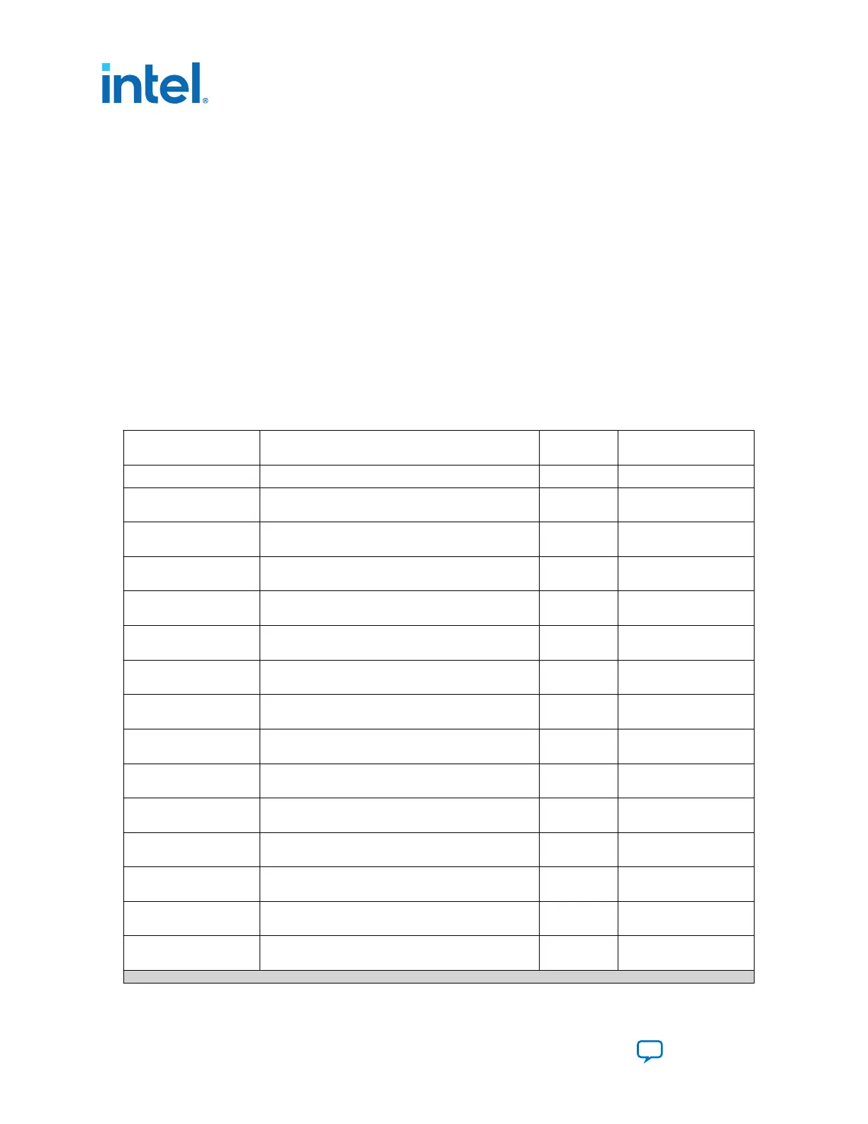
Table 33. FMC A Connector Pin Assignments, Schematic Signal Names
Board Reference Schematic Signal Name FPGA Pin
Number
I/O Standard
D1 FMCA_C2M_PG — —
H5 FMCA_CLK_M2C_N0 AY19 High Speed Differential
I/O
G3 FMCA_CLK_M2C_N1 BA13 High Speed Differential
I/O
H4 FMCA_CLK_M2C_P0 AY20 High Speed Differential
I/O
G2 FMCA_CLK_M2C_P1 BA12 High Speed Differential
I/O
C3 FMCA_DP_C2M_N0 BC8 High Speed Differential
I/O
A23 FMCA_DP_C2M_N1 BD6 High Speed Differential
I/O
A27 FMCA_DP_C2M_N2 BB6 High Speed Differential
I/O
A31 FMCA_DP_C2M_N3 BC4 High Speed Differential
I/O
A35 FMCA_DP_C2M_N4 BB2 High Speed Differential
I/O
A39 FMCA_DP_C2M_N5 BA4 High Speed Differential
I/O
B37 FMCA_DP_C2M_N6 AY2 High Speed Differential
I/O
B33 FMCA_DP_C2M_N7 AW4 High Speed Differential
I/O
B29 FMCA_DP_C2M_N8 AV2 High Speed Differential
I/O
B25 FMCA_DP_C2M_N9 AU4 High Speed Differential
I/O
continued...
6. Board Components
683526 | 2023.07.12
Intel
®
Arria
®
10 FPGA Development Kit User Guide
Send Feedback
86