6.8. Memory
This section describes the development board's memory interface support and also
their signal names, types, and connectivity relative to the FPGA.
6.8.1. Flash
The Arria 10 GX FPGA development board supports two 1 Gb CFI-compatible
synchronous flash devices for non-volatile storage of FPGA configuration data, board
information, test application data, and user code space. These devices are part of the
shared FM bus that connects to the flash memory and MAX V CPLD EPM2210 System
Controller.
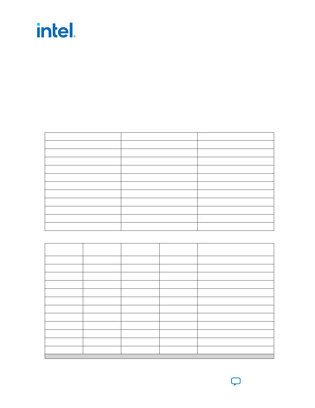
Table 41. Default Memory Map of two 1-Gb CFI Flash Devices
Block Description Size (KB) Address Range
Board test system scratch 512 0x0a10.0000 - 0x0a17.FFFF
User software 14, 336 0x0930.0000 - 0x0A0F.FFFF
Factory software 8, 192 0x08b0.0000 - 0x092F.FFFF
Zips (html, web content) 8, 192 0x0830.0000 - 0x08AF.FFFF
User hardware2 44, 032 0x0580.0000 – 0x082F.FFFF
User hardware1 44, 032 0x02D0.0000 – 0x057F.FFFF
Factory hardware 44, 032 0x0020.0000 – 0x02CF.FFFF
PFL option bits 512 0x0018.0000 – 0x001F.FFFF
Board information 512 0x0010.0000 – 0x0017.FFFF
Ethernet option bits 512 0x0008.0000 – 0x000F.FFFF
User design reset vector 512 0x0000.0000 – 0x0007.FFFF
Table 42. Flash Pin Assignments, Schematic Signal Names, and Functions
Board Reference Schematic Signal
Name
FPGA Pin Number I/O Standard Description
F6 FLASH_ADVN BB22 1.8 V Address valid
B4 FLASH_CEN1 BB23 1.8 V Chip enable
E6 FLASH_CLK BB25 1.8 V Clock
F8 FLASH_OEN BC26 1.8 V Output enable
F7 FLASH_RDYBSYN1 AV23 1.8 V Ready
D4 FLASH_RESETN BA23 1.8 V Reset
G8 FLASH_WEN BD26 1.8 V Write enable
C6 FLASH_WPN — 1.8 V Write protect
A1 FM_A1 AM11 1.8 V Address bus
B1 FM_A2 AM12 1.8 V Address bus
C1 FM_A3 AL12 1.8 V Address bus
D1 FM_A4 AN13 1.8 V Address bus
continued...
6. Board Components
683526 | 2023.07.12
Intel
®
Arria
®
10 FPGA Development Kit User Guide
Send Feedback
102

 Loading...


