6. Board Components
This chapter introduces all the important components on the development kit board.
A complete set of schematics, a physical layout database, and GERBER files for the
development board reside in the development kit documents directory.
6.1. Board Overview
This section provides an annotated board image and the major component
descriptions.
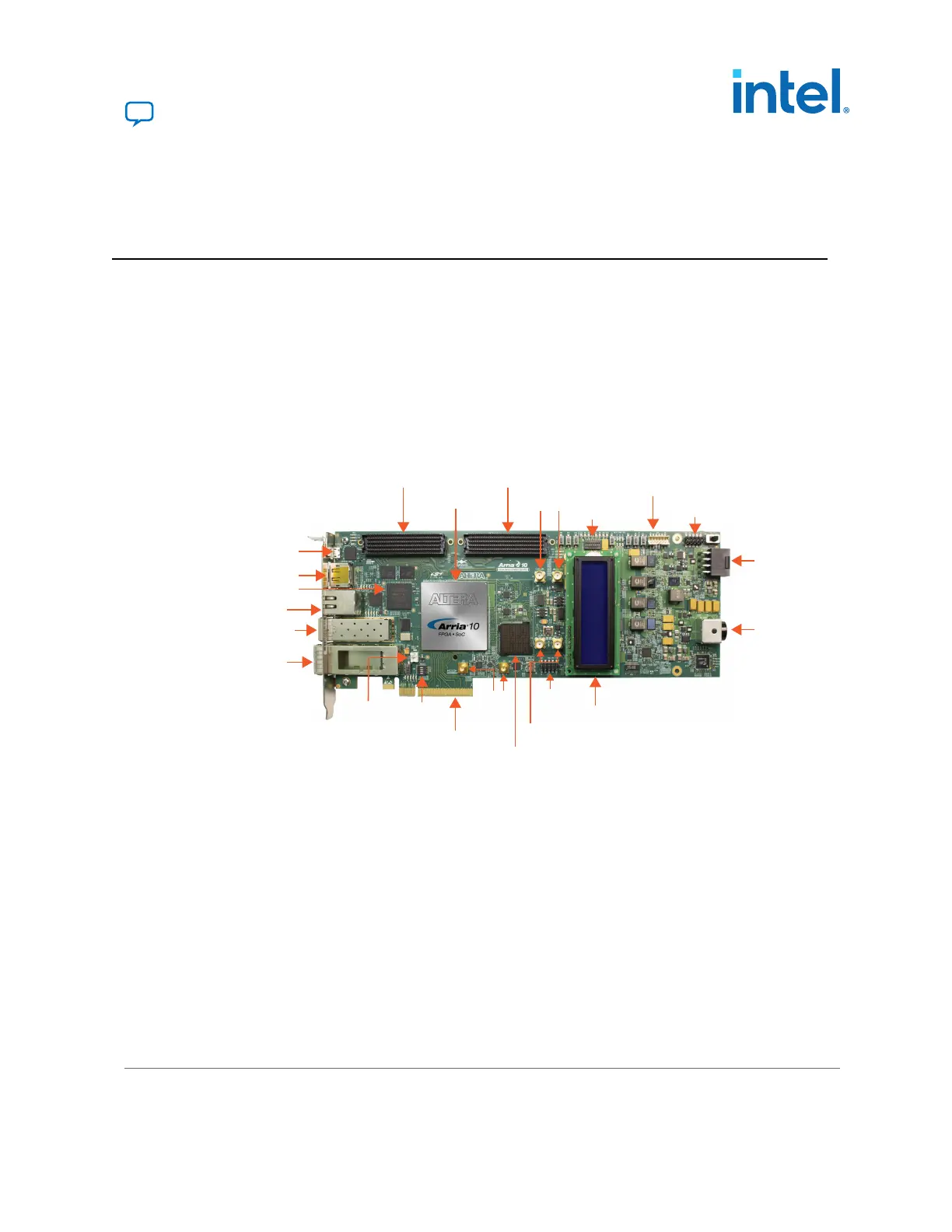
Figure 30. Overview of the Development Board Features (ES Edition)
FMCA (J1)
FMCB (J2)
Arria 10
FPGA (U28)
Clock In/Out
SMA (J6, J7)
User Dipswitch
(SW2)
Power Switch
(SW1)
PCIe ATX
Connector
(J4)
DC Input Jack
(J13)
JTAG Header
(J17)
Character LCD
(B2)
Transceiver TX
(J15, J16)
HiLo Connector
(J14)
SDI Video Port
(J20, J21)
PCI Express
Edge Connector
(J22)
PCIe Dipswitch
(SW3)
Fan Power
Header (J19)
On-Board
USB-Blaster II (J3)
DisplayPort
Connector (J5)
MAX V CPLD (U16)
Gbps Ethernet
Port (J9)
QSFP
Interface (J18)
LTPowerPlay interface
Connector (J24)
SFP+ Interface (J12)
683526 | 2023.07.12
Send Feedback
Intel Corporation. All rights reserved. Intel, the Intel logo, and other Intel marks are trademarks of Intel
Corporation or its subsidiaries. Intel warrants performance of its FPGA and semiconductor products to current
specifications in accordance with Intel's standard warranty, but reserves the right to make changes to any
products and services at any time without notice. Intel assumes no responsibility or liability arising out of the
application or use of any information, product, or service described herein except as expressly agreed to in
writing by Intel. Intel customers are advised to obtain the latest version of device specifications before relying
on any published information and before placing orders for products or services.
*Other names and brands may be claimed as the property of others.
ISO
9001:2015
Registered