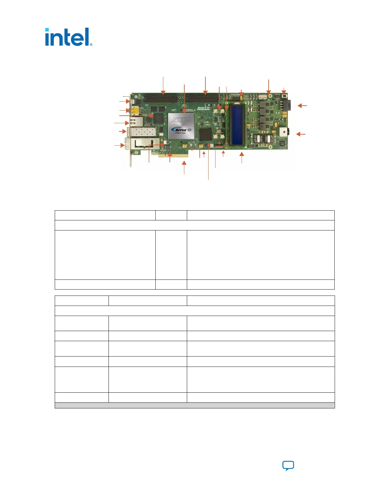
Figure 31. Overview of the Development Board Features
FMCA (J1)
FMCB (J2)
Arria 10
FPGA (U28)
Clock In/Out
SMA (J6, J7)
User Dipswitch
(SW2)
Power Switch
(SW1)
PCIe ATX
Connector
(J4)
DC Input Jack
(J13)
JTAG Header
(J17)
Character LCD
(B2)
Transceiver TX
(J15, J16)
HiLo Connector
(J14)
SDI Video Port
(J20, J21)
PCI Express
Edge Connector
(J22)
PCIe Dipswitch
(SW3)
Fan Power
Header (J19)
On-Board
USB-Blaster II (J3)
DisplayPort
Connector (J5)
MAX V CPLD (U16)
Gbps Ethernet
Port (J9)
QSFP
Interface (J18)
LTPowerPlay interface
Connector (J24)
SFP+ Interface (J12)
Table 15. Arria 10 GX FPGA Development Board Components
Board Reference Type Description
Featured Devices
U28 FPGA Arria 10 GX FPGA, 10AX115S2F45I1SG:
• Adaptive logic modules (ALMs): 427,200
• LEs (K): 1,150
• Registers: 1,708,800
• M20K memory blocks: 2,713
• Transceiver count: 96
• Package Type: 1932 BGA
U16 CPLD MAX V CPLD, 2210 LEs, 256FBGA 1.8V VCCINT
Board Reference Type Description
Configuration and Setup Elements
J3 On-Board USB-Blaster II Micro-USB 2.0 connector for programming and debugging the
FPGA.
SW3 PCI Express Control DIP switch Enables PCI Express link widths x1, x4, and x8.
SW4 JTAG Bypass DIP switch Enables and disables devices in the JTAG chain. This switch is
located on the back of the board.
SW5 FPP Configuration DIP Switch
Sets the Arria 10 MSEL pins and VID_EN pin.
SW6 Board settings DIP switch Controls the MAX V CPLD System Controller functions such as
clock select, clock enable, factory or user design load from flash
and FACTORY signal command sent at power up. This switch is
located at the bottom of the board.
S4 CPU reset push button The default reset for the FPGA logic.
continued...
6. Board Components
683526 | 2023.07.12
Intel
®
Arria
®
10 FPGA Development Kit User Guide
Send Feedback
56
 Loading...


