Schematics, Component Location Diagrams, and Parts Lists: List of Schematics, Component Location Diagrams, and Parts Lists 7-1
6815854H01-A June 16, 2005
Chapter 7 Schematics, Component Location Diagrams, and Parts Lists
7.1 List of Schematics, Component
Location Diagrams, and Parts
Lists
The following table lists the schematics,
component location diagrams, and parts lists
contained in this chapter.
Table 7-1. List of Schematics, Component Location
Diagrams, and Parts Lists
Figure Title Page
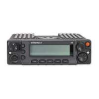
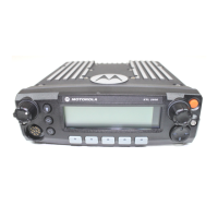
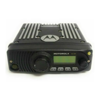
Control Head
Control Head Board Overall Block Diagram 7-3
Control Head Controller, OMAP Processor)
( Sheet 1 of 2)
7-4
Control Head Controller, OMAP Processor
(Sheet 2 of 2)
7-5
Control Head Controller (SDRAM and Flash
Memory)
7-6
TPS65012 Power Management IC, Factory
Programming
7-7
Voltage Regulators 7-8
AVR Power Management Control 7-9
GCAI Accessory Interface (Sheet 1of 2) 7-10
GCAI Accessory Interface (Sheet 2 of 2) 7-11
GCAI Connector Schematic 7-12
User Interface (Sheet 1 of 2) 7-13
User Interface (Sheet 2 of 2) 7-14
Rear Connector 7-15
Control Head Main Board Layout—Side 1 Top 7-16
Control Head Main Board Layout—Side 2 Bottom 7-17
Control Head Main Board Parts List 7-18
GCAI Connector Board Layout—Side 1 Top 7-23
GCAI Connector Board Layout—Side 2 Bottom 7-24
GCAI Connector Board Parts List 7-25
VHF
HUD4022A Main Board Overall Block Diagram and
Interconnections
7-26
HUD4022A Controller Block Diagram and
Interconnections (Sheet 1 of 2)
7-27
HUD4022A Controller Block Diagram and
Interconnections (Sheet 2 of 2)
7-28
HUD4022A Controller Urchin IC, MUX, and
AD5320 DAC Schematic
7-29
HUD4022A Controller Audio Schematic 7-30
HUD4022A Controller Power Control (Sheet 1 of 2) 7-31
HUD4022A Controller Power Control (Sheet 2 of 2) 7-32
HUD4022A Frequency Generation Unit Overall
Schematic (Sheet 1 of 2)
7-33
HUD4022A Frequency Generation Unit Overall
Schematic (Sheet 2 of 2)
7-34
HUD4022A VHF Transmitter VCO Schematic 7-35
HUD4022A Frequency Generation Unit VHF
Receive Injection Schematic
7-36
HUD4022A Frequency Generation Unit VHF
Transmit Injection Schematic
7-37
HUD4022A Receiver Back-End Schematic 7-38
HUD4022A Receiver Front-End Schematic (Sheet
1 of 2)
7-39
HUD4022A Receiver Front-End Schematic (Sheet
2 of 2)
7-40
HUD4022A Receiver IF Schematic 7-41
HUD4022A RF Power Amplifier (RFPA) Schematic
(Sheet 1 of 2)
7-42
HUD4022A RF Power Amplifier (RF PA) Schematic
(Sheet 2 of 2)
7-43
HUD4022A Secure Block Diagram and
Interconnections
7-44
HUD4022A Accessory Connector Schematic 7-45
HUD4022A Power Supply Schematic 7-46
HUD4022A USB/RS232/SB9600 Schematic 7-47
Table 7-1. List of Schematics, Component Location
Diagrams, and Parts Lists (Continued)
Figure Title Page
HUD4022A SB9600 Schematic 7-48
HUD4022A USB/RS232/SB9600 VIP Input/Output
Schematic
7-49
HUD4022A Control-Head Connector Schematic 7-50
Interface Connector Schematic 7-51
HUD4022A Main Board Layout—Side 1 Top 7-52
HUD4022A Main Board Layout—Side 1 Bottom 7-53
HUD4022A Main Board Layout—Side 2 Top 7-54
HUD4022A Main Board Layout—Side 2 Bottom 7-55
HUD4022A Main Board Parts List 7-56
UHF Range 1
HUE4039A Main Board Overall Block Diagram and
Interconnections
7-65
HUE4039A Controller Block Diagram and
Interconnections (Sheet 1 of 2)
7-66
HUE4039A Controller Block Diagram and
Interconnections (Sheet 2 of 2)
7-67
HUE4039A Controller URCHIN IC, MUX, and
AD5320 DAC Schematic
7-68
HUE4039A Controller Audio Schematic 7-69
HUE4039A Controller Power Control Schematic 7-70
HUE4039A Frequency Generation Unit Schematic 7-71
HUE4039A Receive VCO Schematic 7-72
HUE4039A Transmit VCO Schematic 7-73
HUE4039A Receiver Back-End Schematic 7-74
HUE4039A Receiver Front-End Schematic 7-75
HUE4039A Receiver Mixer Schematic 7-76
HUE4039A Receiver Preselector Schematic 7-77
HUE4039A Receiver IF Schematic 7-78
HUE4039A RF Power Amplifier (RF PA) Schematic 7-79
HUE4039A Output Network (ON) Schematic 7-80
HUE4039A Secure Block Diagram and
Interconnections
7-81
HUE4039A Rear Accessory Connector Schematic 7-82
Table 7-1. List of Schematics, Component Location
Diagrams, and Parts Lists (Continued)
Figure Title Page
HUE4039A Secure Power Supply Schematic 7-83
HUE4039A Secure USB/RS232/SB9600
Schematic
7-84
HUE4039A Secure SB9600 Schematic 7-85
HUE4039A Secure USB/RS232/SB9600 VIP Input/
Output Schematic
7-86
HUE4039A Secure Control-Head Connector
Schematic
7-87
HUE4039A Secure Interface Connector Schematic 7-88
HUE4039A Main Board Layout—Side 1 Top 7-89
HUE4039A Main Board Layout—Side 1 Middle 7-90
HUE4039A Main Board Layout—Side 1 Bottom 7-91
HUE4039A Main Board Layout—Side 2 Top 7-92
HUE4039A Main Board Layout—Side 2 Middle 7-93
HUE4039A Main Board Layout—Side 2 Bottom 7-94
HUE4039A Main Board Parts List 7-95
UHF Range 2
HUE4040A Main Board Overall Block Diagram and
Interconnections
7-106
HUE4040A Controller Block Diagram and
Interconnections (Sheet 1 of 2)
7-107
HUE4040A Controller Block Diagram and
Interconnections (Sheet 2 of 2)
7-108
HUE4040A Controller URCHIN IC, MUX, and
AD5320 DAC Schematic
7-109
HUE4040A Controller Audio Schematic 7-110
HUE4040A Controller Power Control Schematic 7-111
HUE4040A Frequency Generation Unit Schematic 7-112
HUE4040A Receive VCO Schematic 7-113
HUE4040A Transmit VCO Schematic 7-114
HUE4040A Receiver Back-End Schematic 7-115
HUE4040A Receiver Front-End Schematic 7-116
HUE4040A Receiver Mixer Schematic 7-117
HUE4040A Receiver Preselector Schematic 7-118
Table 7-1. List of Schematics, Component Location
Diagrams, and Parts Lists (Continued)
Figure Title Page

 Loading...