USB and PCIe
NVIDIA Jetson Xavier NX DG-09693-001_v1.7 | 27
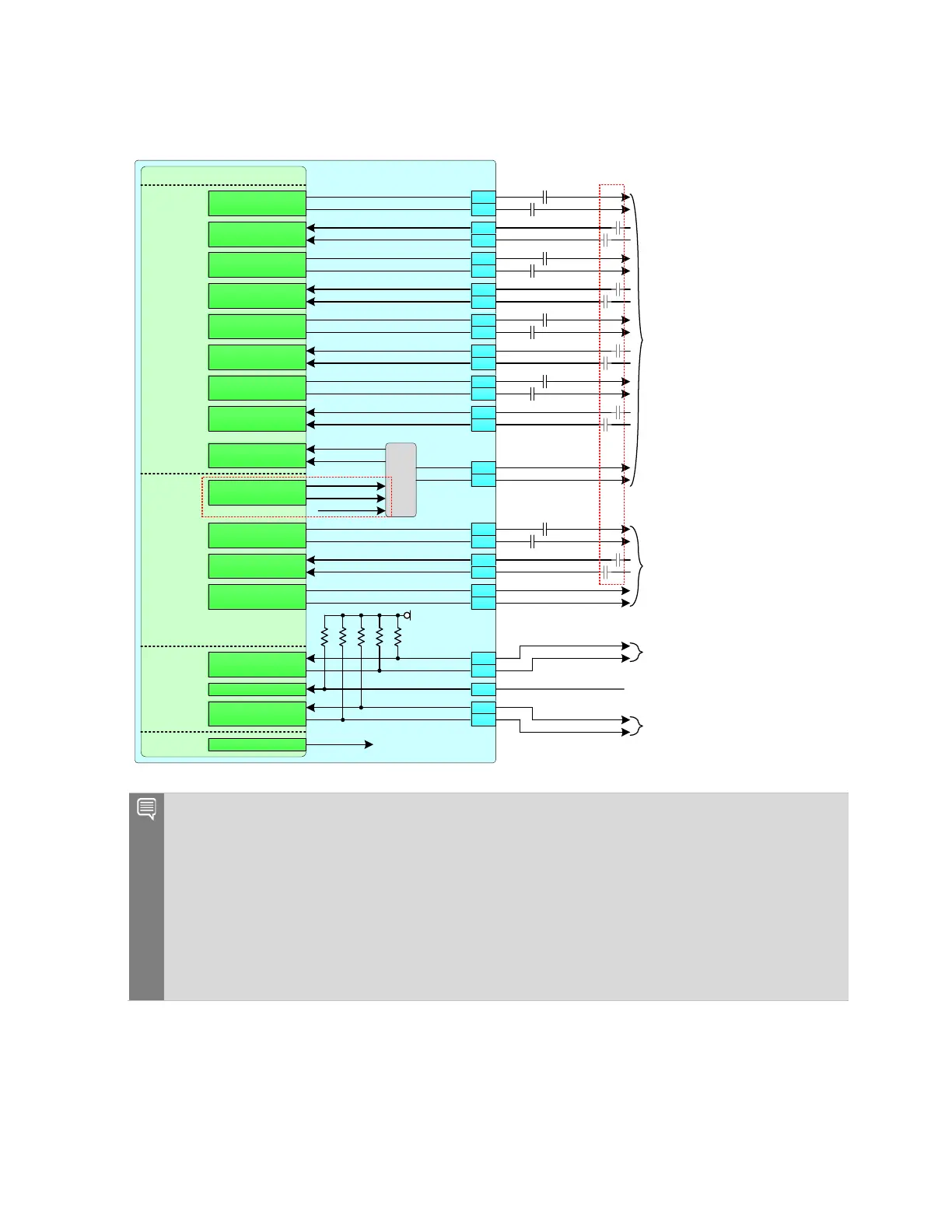
Figure 6-9. PCIe Root Port Connections Example
Jetson
SoC - PCIe
NVHS
PEX_L5_CLKREQ_N
PEX_L5_RST_N
PEX_WAKE_N
PEX
Control
NVHS_
TX3_N
NVHS_TX3_P
PCIe 0 Lane 3
PCIe 0 Lane 2
PCIe 0 Lane 1
PCIe 0 Lane 0
NVHS_RX3_N
NVHS_RX3_ P
NVHS_
TX2_N
NVHS_T
X2_P
NVHS_RX2_N
NVHS_R
X2_P
NVHS_TX1_N
NVHS_TX1_P
NVHS_
RX1_N
NVHS_R
X1_P
NVHS_TX0_N
NVHS_T
X0_P
NVHS_RX0_N
NVHS_R
X0_P
PCIE0_TX3_N
PCIE0_TX3_P
PCIE0_RX3_N
PCIE0_RX3_P
PCIE0_TX2_N
PCIE0_TX2_P
PCIE0_RX2_N
PCIE0_RX2_P
PCIE0_TX1_N
PCIE0_TX1_P
PCIE0_RX1_N
PCIE0_RX1_P
PCIE0_TX0_N
PCIE0_TX0_P
PCIE0_RX0_N
PCIE0_RX0_P
PCIE0_CLK_N
PCIE0_CLK_P
PCIE1_TX0_N
PCIE1_TX0_P
PCIE1_RX0_N
PCIE1_RX0_P
PCIE1_CLK_N
PCIE1_CLK_P
PCIE1_CLKREQ*
PCI E 1_R ST*
PCIE_WAKE*
PCIE0_CLKREQ*
PCI E 0_R ST*
3.3V
180
181
179
PCIe 0 (Ctrl #5) –
PCIe x4 conn/device
(i.e. M.2 Key M)
100kΩ
4.7kΩ
47kΩ
156
154
155
157
148
150
149
151
140
142
137
139
134
136
131
133
PEX_CLK4_ N
PEX_CLK4_ P
PEX_RX11_N
PEX_RX11_P
167
169
173
175
PCIe 0 (Ctrl #5) –
PCIe x4 conn/device
(i.e. M.2 Key M)
PEX_TX11_N
PEX_TX11_P
172
174
PCIe 1 Lane 0
PCIe 0 (Ctrl #4)
–
PCIe x1 conn/device
(i.e. M.2 Key E)
PEX_L4_CLKREQ_N
PEX_L4_RST_N
182
183
PCIe 1 (Ctrl #4) –
PCIe x1 conn/device
(i.e. M.2 Key E)
4.7kΩ
47kΩ
Shared wake pin
PEX
162
NVHS0_REFCLK_N
NVHS0_REFCLK_P
160
PEX_CLK5_ N
PEX_CLK5_ P
Mux
SE L
AO_HV
CAN0_EN
CAN0_EN
NVHS0_REFCL K/P EX_CL K5
Mux Con tro l
Se e No te 1
Se e No te 2
Notes:
1. For Root Port operation, the mux should be set to output the PEX_CLK5 signals. CAN0_EN
which is used for the mux select should be set low.
2. AC Capacitors required on RX lines on carrier board if connected directly to device. They
should not be on the carrier board if connected to PCIe connector, M.2 Key M, etc. In those
cases, the AC caps are on the board connected to those connectors.
3. See design guidelines for correct AC capacitor values.
4. The PCIe REFCLK inputs and PCIEx_CLK clock outputs comply to the PCIe CEM specification
“REFCLK DC Specifications and AC Timing Requirements.” The clocks are HCSL compatible.
Figure 6-10 shows the x4 interface configured as Endpoint for the PCIe Endpoint connections.

 Loading...


