USB and PCIe
NVIDIA Jetson Xavier NX DG-09693-001_v1.7 | 18
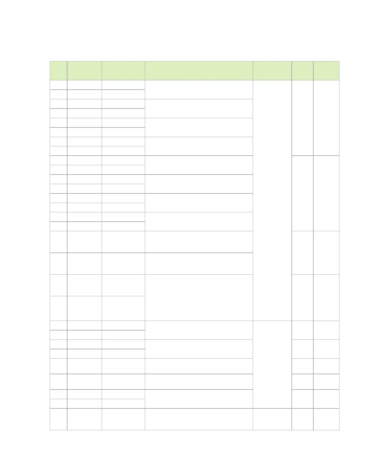
Table 6-2. USB 3.2 and PCIe Pin Description
Pin #
Module Pin
Xavier Signal Usage/Description
Recommended
Directio
Pin Type
131 PCIE0_RX0_N NVHS0_RX0_N
PCIe #0 Receive 0 (PCIe Ctrl #5 Lane 0)
PCIe x4
conn/device (i.e.
M.2 Key M)
Input PCIe PHY
133 PCIE0_RX0_P NVHS0_RX0_P
137 PCIE0_RX1_N NVHS0_RX1_N
PCIe #0 Receive 1 (PCIe Ctrl #5 Lane 1)
139 PCIE0_RX1_P NVHS0_RX1_P
149 PCIE0_RX2_N NVHS0_RX2_N
PCIe #0 Receive 2 (PCIe Ctrl #5 Lane 2)
151 PCIE0_RX2_P NVHS0_RX2_P
155 PCIE0_RX3_N NVHS0_RX3_N
PCIe #0 Receive 3 (PCIe Ctrl #5 Lane 3)
157 PCIE0_RX3_P NVHS0_RX3_P
134 PCIE0_TX0_N NVHS0_TX0_N
PCIe #0 Transmit 0 (PCIe Ctrl #5 Lane 0)
Output PCIe PHY
136 PCIE0_TX0_P NVHS0_TX0_P
140 PCIE0_TX1_N NVHS0_TX1_N
PCIe #0 Transmit 1 PCIe Ctrl #5 Lane 1)
142 PCIE0_TX1_P NVHS0_TX1_P
148 PCIE0_TX2_N NVHS0_TX2_N
PCIe #0 Transmit 2 (PCIe Ctrl #5 Lane 2)
150 PCIE0_TX2_P NVHS0_TX2_P
154 PCIE0_TX3_N NVHS0_TX3_N
PCIe #0 Transmit 3 (PCIe Ctrl #5 Lane 3)
156 PCIE0_TX3_P NVHS0_TX3_P
181 PCIE0_RST* PEX_L5_RST_N
PCIe #0 Reset (PCIe Ctrl #5). 4.7kΩ pull-up to
3.3V on the module. Output when module is Root
Port - input when module Endpoint.
Bidir
Open
Drain 3.3V
180
PCIE0_CLKRE
Q*
PEX_L5_CLKREQ_
N
PCIE #0 Clock Request (PCIe Ctrl #5). 47kΩ pull-
up to 3.3V on the module. Input when module is
Root Port - output when module is Endpoint.
160 PCIE0_CLK_N
PEX_CLK5N or
NVHS0_REFCLK_
N
PCIe #0 Reference Clock controlled by on-
module mux by SoC CAN0_EN. When CAN0_EN
is low, PEX_CLK5 is selected (reference clock
when module is Root Port). When CAN0_EN is
high, NVHS0_REFCLK is selected (reference
clock input when Jetson Xavier NX is an
Endpoint).
Bidir PCIe PHY
162 PCIE0_CLK_P
PEX_CLK5P or
NVHS0_REFCLK_
P
167 PCIE1_RX0_N PEX_RX11_N
PCIe #1 Receive 0 (PCIe Ctrl #4 Lane 0)
PCIe x1
conn/device (i.e.
M.2 Key E)
Input PCIe PHY
169 PCIE1_RX0_P PEX_RX11_P
172 PCIE1_TX0_N PEX_TX11_N
PCIe #1 Transmit 0 (PCIe Ctrl #4 Lane 0) Output PCIe PHY
174 PCIE1_TX0_P PEX_TX11_P
183 PCIE1_RST* PEX_L4_RST_N
PCIe #1 Reset (PCIe Ctrl #4). 4.7kΩ pull-up to
3.3V on the module.
Output
Open
Drain 3.3V
182
PCIE1_CLKRE
Q*
PEX_L4_CLKREQ_
N
PCIE #1 Clock Request (PCIe Ctrl #4). 47kΩ pull-
up to 3.3V on the module.
Bidir
Open
Drain 3.3V
173 PCIE1_CLK_N PEX_CLK4N
PCIe #1 Reference Clock (PCIe Ctrl #4) Output PCIe PHY
175 PCIE1_CLK_P PEX_CLK4P
179 PCIE_WAKE* PEX_WAKE_N PCIe Wake. 47kΩ pull-up to 3.3V on the module.
Shared between
x1 and x4 PCIe
interfaces.
Input
Open
Drain 3.3V

 Loading...


