MIPI CSI Video Input
NVIDIA Jetson Xavier NX DG-09693-001_v1.7 | 60
Max intra-pair skew 1 ps
Max trace delay skew between DQ and CLK
1 / 1.5 / 2.5 Gbps
40 / 26.7 / 16
ps
includes all the data lines
associated with a single clock. This may
be 2 differential data lanes for a x2
interface, or 4 differential data lanes for
a x4 interface.
Keep critical traces away from other signal traces or unrelated power traces/areas or power supply components
Note: Any EMI/ESD devices must be tuned to minimize impact to signal quality and meet the timing and Vil/Vih requirements at
the receiver and maintain signal quality and meet requirements for the frequencies supported by the design.
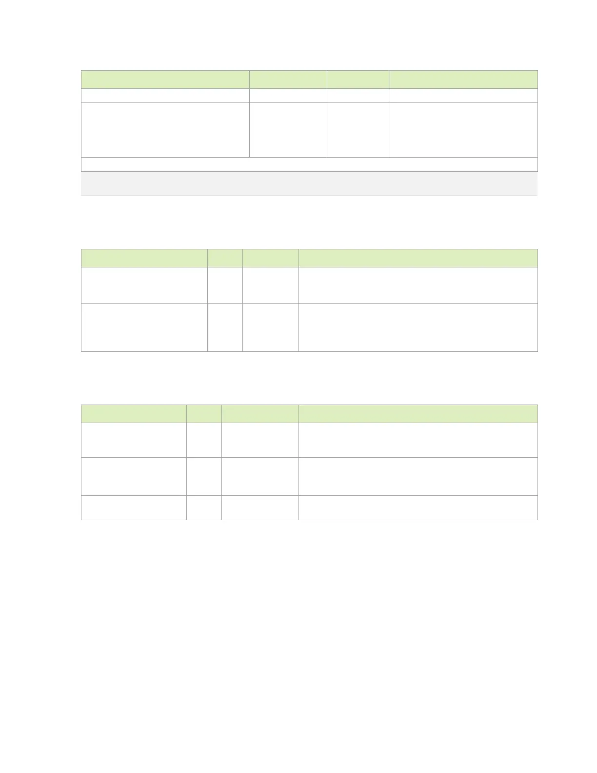
Table 9-5. MIPI CSI Signal Connections
CSI[4:0]_CLK_N/P Camera
#[5:1]
DSI_CLK_N/P Camera #6
I See note CSI Differential Clocks: Connect to clock pins of camera. See
Table 9-3 for details
CSI[3:0]_D[1:0]_N/P Camera
#[4:1]
CSI4_D[3:0]_N/P Camera #5
DSI_D[1:0]_N/P Camera #6
I/O See note
CSI Differential Data Lanes: Connect to data pins of camera. See
Table 9-3 for details
Table 9-6. Miscellaneous Camera Connections
CAM_I2C_CLK
CAM_I2C_DAT
O
I/O
2.2kΩ pull-ups
VDD_3V3_SYS (on
Jetson Xavier NX).
Camera I2C Interface: Connect to I2C SCL and SDA pins of
imager.
CAM[1:0]_MCLK
GPIO01 (opt. MCLK2)
GPIO11 (opt. MCLK3)
O Camera Clocks: Connect to camera reference clock inputs.
CAM[1:0]_PWDN O
Camera Power Control signals (or GPIOs [1:0]): Connect to
power down pins on camera(s).

 Loading...


