MIPI CSI Video Input
NVIDIA Jetson Xavier NX DG-09693-001_v1.7 | 59
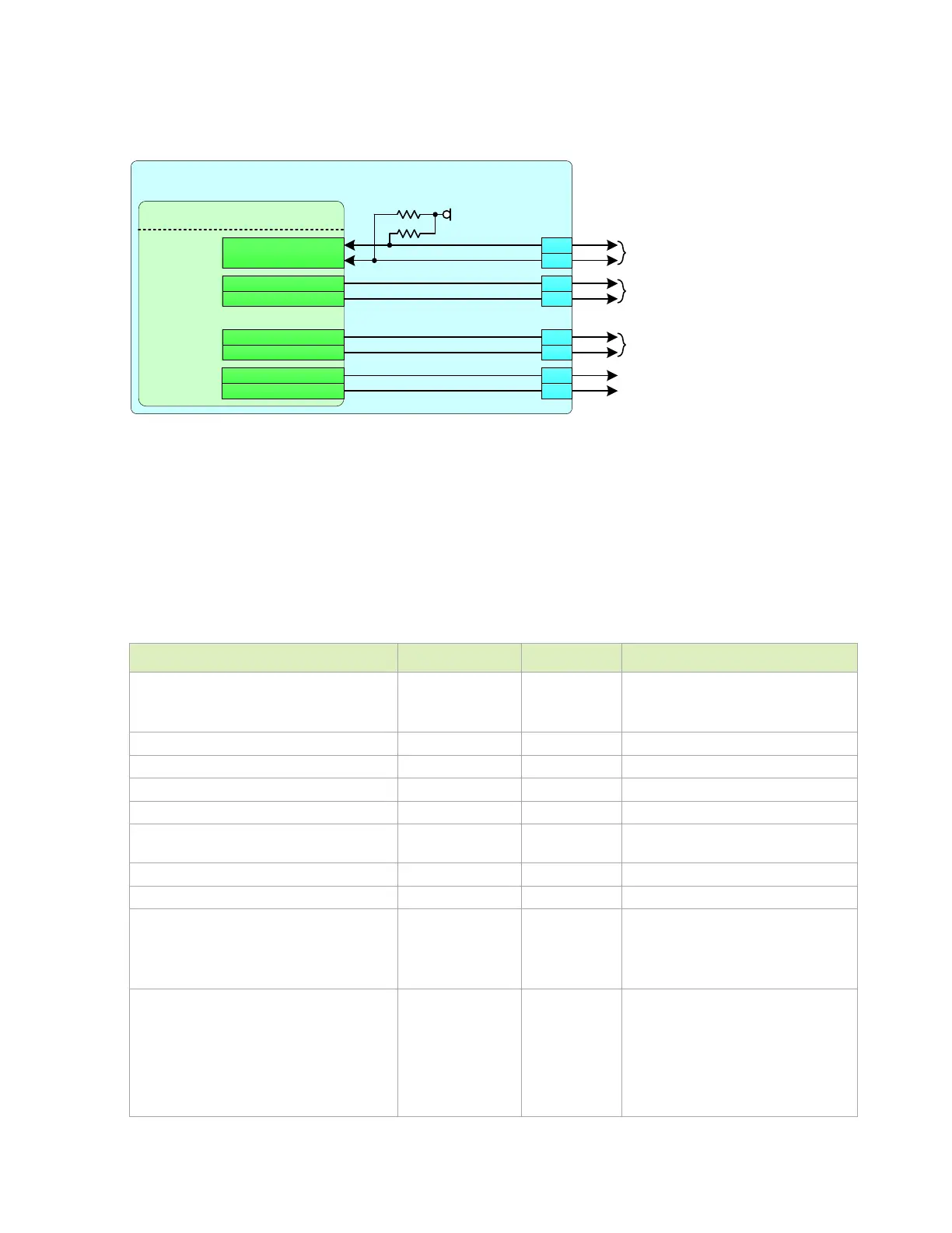
Figure 9-3. Available Camera Control Pins
Jetson
SoC
CAM
CAM_I2C_SCL
CAM_I2C_SDA
EXTPERIPH1_CLK
EXTPERIPH2_CLK
SOC_GPIO04
SOC_GPIO05
2. 2kΩ
2. 2kΩ
VDD_3V3_SY S
Camera
I2C
Camera 0
Clock/Control
Camera 1
Clock/Control
CAM_I2C_SCL
CAM_I2C_SDA
CAM0_MCLK
CAM0_PWDN
CAM1_MCLK
CAM1_PWDN
GP IO 01
GP IO 11
215
116
114
213
120
122
SOC_GPIO41
Camera 2 Clock
Camera 3 Clock
216
118
SOC_GPIO42
9.1 CSI Design Guidelines
The following tables describe the design guidelines for the CSI design.
Table 9-4. MIPI CSI Interface Signal Routing Requirements
Max Data Rate (per data lane) for High-Speed
mode
Max Frequency (for Low Power mode)
10
MHz
Number of loads 1 load
Reference plane
GND
Trace impedance: Diff pair / SE 90-100 / 45-50 Ω ±10%
Via proximity (signal to reference) < 0.65 (3.8) mm (ps)
Intra-pair trace spacing 0.15mm mm Can be adjusted to meet Differential
Impedance.
Trace spacing: Microstrip / Stripline 2x / 2x dielectric
Max PCB breakout delay 48 ps
Max Insertion loss
1 Gbps
1.5 Gbps
2.5 Gbps
3.00
2.90
1.92
dB
Max trace delay / length
1 Gbps (Stripline/Microstrip)
1.5 Gbps
2.5 Gbps
2526 (421) / 2487
(421)
1913 (319) / 1885
(319)
900 (150) / 886
(150)
ps (mm)

 Loading...


