Display
NVIDIA Jetson Xavier NX DG-09693-001_v1.7 | 47
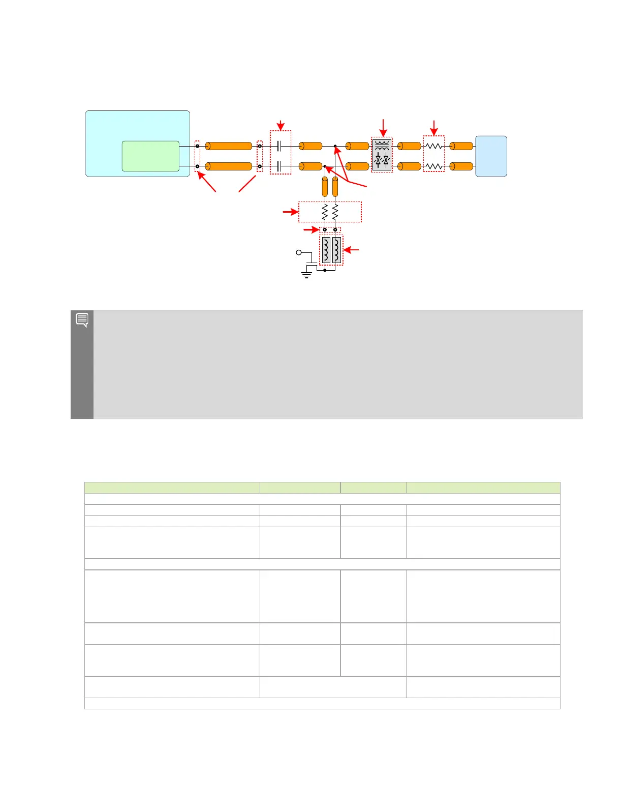
Figure 8-8. HDMI Clk and Data Topology
100Ω*
100Ω*
100Ω*
100Ω*
100Ω*
100Ω*
Jetson
HDMI
Conn
AC
C AP
Se g D Se g F
MOD_SLEE P*
49 9Ω,
1%
PCB Vias
PCB Vias
0. 1u F
0. 1u F
R
PD
Comm on Mode
Chokes & ES D
Se e No te 1
49 9Ω,
1%
Se g B Se g E
Se g C
SoC
95-100Ω 100Ω*
95-100Ω 100Ω*
Main Route –
Se g A
* Note 3 * Note 3* Note 3 * Note 3
R
S
(See Not e 4 )
Choke or Trace
Se e No te 2
Notes:
1. RPD pad must be on the main trace. RPD and ACCAP must be on same layer.
2. Chokes (600 Ω @ 100 MHz) or narrow traces (1 uH @ DC-100 MHz) between pull-downs and FET are
chokes between pull-downs and FET are optional improvements for HDMI 2.0 operation.
3. The trace after the main route via should be routed on the top or bottom layer of the PCB, and either
with 100 ohm differential impedance, or as uncoupled 50 ohm SE traces.
4. RS series resistor is required to meet HDMI 2.0 compliance. See the RS section in Table 8-5 for details.
Table 8-5. HDMI Interface Signal Routing Requirements
Per lane – not total link bandwidth
Unidirectional, differential
At receiver
100
Ω
Differential To 3.3V at receiver
To
near connector
<= 2
<= 3
< 6
dB @ 1.5GHz
dB @ 3GHz
dB @ 6GHz
10%-90%. If TDR dip is 75~85ohm that
dip width should < 250ps
<= -40
dB at 3GHz
PSNEXT is derived from an algebraic
summation of the individual NEXT effects
on each pair by the other pairs
IL/FEXT plot: See HDMI Guideline
Figure 8-9
TDR plot: See Figure 8-10

 Loading...


