USB and PCIe
NVIDIA Jetson Xavier NX DG-09693-001_v1.7 | 32
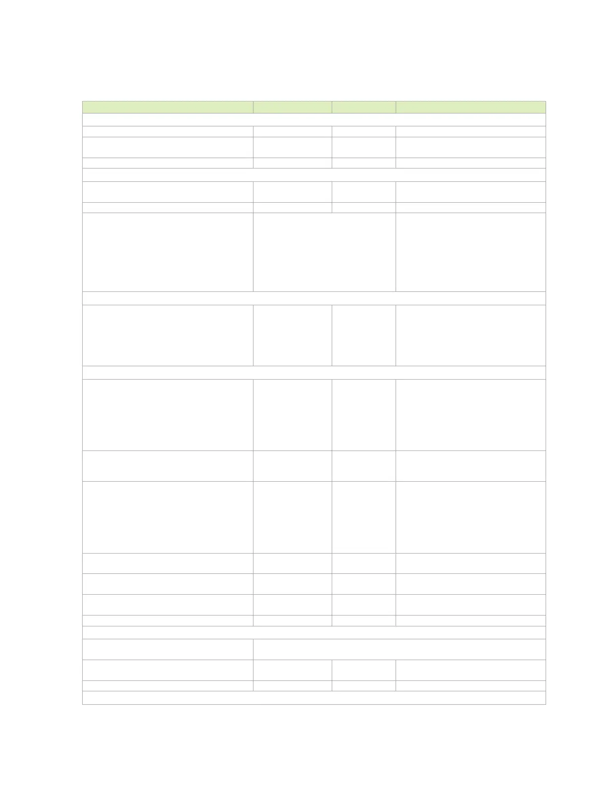
Table 6-10. PCIe Gen4 Interface Signal Routing Requirements
8.0GHz, half-rate architecture
Unidirectional, differential. Driven by
100 MHz common reference clock
To GND Single Ended for P and N
Trace Impedance
differential / Single Ended
• Use spread-glass (denser weave)
instead of regular-glass (sparse
weave) to minimize intra-pair skew
• Use zig-zag route instead of
straight to minimize skew, this is a
mandatory for PCIe gen4 design
Trace Spacing (Stripline)
Pair – Pair
To plane and capacitor pad
To unrelated high-speed signals
4x
4x
4x
Dielectric
TX and RX should not be routed on the
same layer. If this is required in a
design, they should not be interleaved,
and the spacing between the closest RX
and TX lanes must be 9x Dielectric
Trace loss budget (for carrier board routing)
Routing direct to device
Routing to PCIe/M.2 connector
-16
-10.5
dB
Loss: GEN4 budget – module – end
device – safety margin (-28dB + 5dB +
4dB + 3dB)
Loss: GEN3 budget – module – end
device – safety margin (-28dB + 5dB +
Breakout region (Max Length) 41.9 ps Minimum width and spacing. 4x or
wider dielectric height spacing is
Direct to device on carrier board
Stripline
Microstrip
Routed to PCIe or M.2 connector
Stripline
11.9 (2070)
10.9 (1630)
7.8 (1360)
in (ps)
Mid-loss PCB of 1.47dB/in (Microstrip)
or 1.35dB/in (Stripline) is used. Also,
175ps/in for Stripline routing and
150ps/in for Microstrip.
Max PCB via distance from the
Device/Connector
Max distance from Device ball or
Connector pin to first PCB via.
PCB within pair (intra-pair) skew
Do trace length matching before hitting
discontinuities.
Within pair (intra-pair) matching between
subsequent discontinuities
Differential pair uncoupled length
Place GND vias as symmetrically as possible to data pair vias. GND via distance
should be placed less than 1x the diff pair via pitch
Use micro via or back drilled via - no via
stub allowed.

 Loading...


