Display
NVIDIA Jetson Xavier NX DG-09693-001_v1.7 | 41
8.1.1 eDP and DP Routing Guidelines
The following routing requirements meet the eDP and DP routing guidelines.
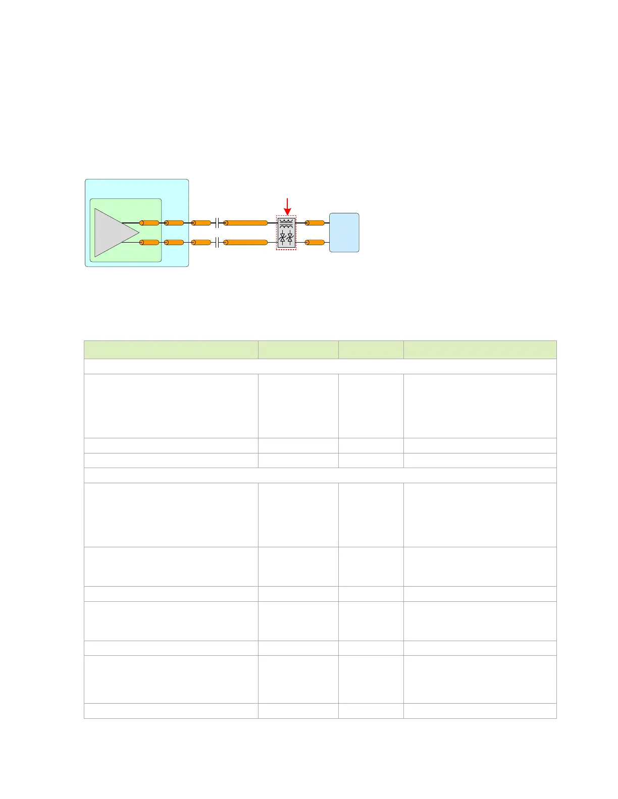
Figure 8-2. eDP and DP Differential Main Link Topology
Jetson
eDP
Conn
SoC
Pkg
DP
Dri ve r
P
N
Comm on Mode
Chokes & ES D
Table 8-3. ePD and DP Main Link Signal Requirements Including
DP_AUX
Max data rate / Min UI
RBR
HBR
HBR2
HBR3
1.6 / 617
2.7 / 370
5.4 / 185
8.1 / 123
Gbps / ps
Per data lane
Number of loads / topology 1 load Point-Point, differential, unidirectional
Termination 100 Ω On die at TX/RX
IL (min)
RBR
HBR
HBR2
HBR3
-0.7
-1.2
-2.4
-4.0
dB @ 0.81GHz
dB @ 1.35GHz
dB @ 2.7GHz
dB @ 4.05GHz
Resonance dip frequency (min)
HBR2
HBR3
8
12
GHz
TDR dip (min) 85 Ω @ Tr-200ps (10%-90%)
FEXT (max) -40
-30
-30
dB @ DC
dB @ 2.7GHz
dB @ 2.7GHz
See Figure 8-3 and TBD
Trace impedance Diff pair 90
85
Ω (±15%) 100Ω is the spec. target.
85Ω is preferable as it can provide
better trace loss characteristic
performance. See Note 1.
Reference plane

 Loading...


