USB and PCIe
NVIDIA Jetson Xavier NX DG-09693-001_v1.7 | 30
GEN1/GEN2: Min/Max
GEN3: Min/Max
0.075 / 0.265
0.176 / 0.265
uF
0.1uF or 0.22uF recommended for
GEN1 or GEN2. 0.22uF recommended
for GEN3. Only required for TX pair
Location (max length to adjacent
discontinuity)
Discontinuity such as edge finger,
component pad
Voiding the plane directly under the
pad 3-4 mils larger than the pad size
Voiding the plane directly under the
pad 5.7 mils larger than the pad size
General: See Chapter 18 for guidelines related to serpentine routing, routing over voids and noise coupling
Notes:
1. The PCIe spec. has 40-60Ω absolute min/max trace impedance, which can be used instead of the 50Ω, ± 15%.
2. If routing in the same layer is necessary, route group TX and RX separately without mixing RX/TX routes and keep distance
between nearest TX/RX trace and RX to other signals 3x RX-RX separation.
3. For trace loss >= 0.7dB/in @ 2.5 GHz, the max trace length should be 7 inches. To reduce trace loss, ensure the loss tangent of
the dielectric material and roughness of the metal are tightly controlled.
4. The average of the differential signals is used for length matching.
5. Do length matching before Via transitions to different layers or any discontinuity to minimize common mode conversion.
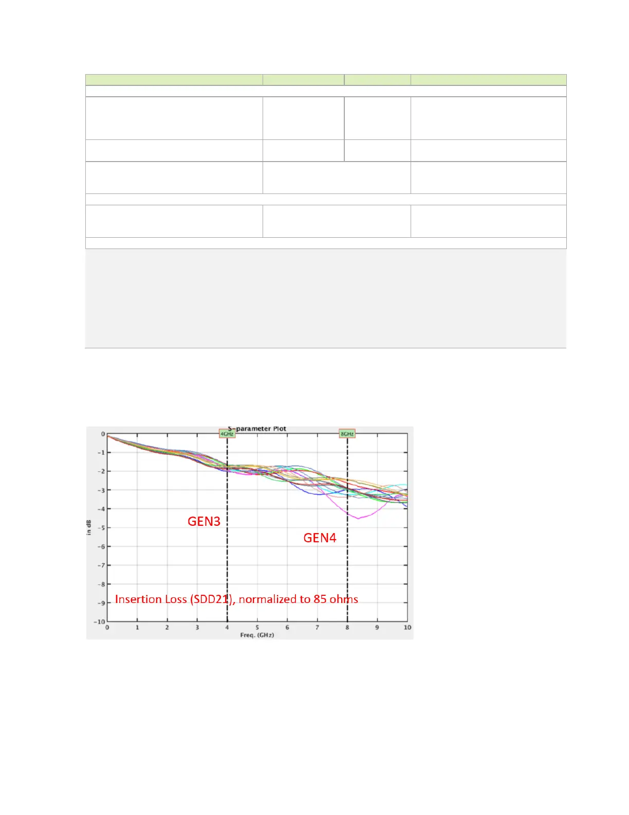
Figure 6-11. Insertion Loss S-Parameter Plot (SDD21)

 Loading...


