Power
NVIDIA Jetson Xavier NX DG-09693-001_v1.7 | 12
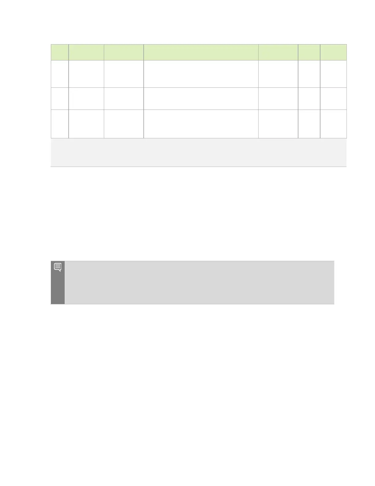
Pin #
Module Pin
Name
Xavier Pin
Name
Usage/Description
Recommended
Usage
Directio
n
Pin Type
when module power sequence is complete. Used
to ensure proper power on/off sequencing between
module and carrier board supplies. 1kΩ pull-up to
1.8V on the module.
178 MOD_SLEEP* SOC_PWR_REQ
Module Sleep. When active (low), indicates module
has gone to Sleep (SC7) mode.
Control of HDMI
See Figure 8-7 .
Output
CMOS –
1.8V
210 CLK_32K_OUT
(PMIC GPIO4
32K CLK Out)
Sleep/Suspend clock
Sleep/suspend
clock for devices
such as M.2 Key
E
Output
CMOS –
1.8V
Notes:
1. In the Type/Dir column, Output is from Jetson Xavier NX. Input is to Jetson Xavier NX. Bidir is for Bidirectional signals.
2. The directions for FORCE_RECOVERY* and SLEEP/WAKE* signals are true when used for those functions. Otherwise as GPIOs,
the direction is bidirectional.
5.1 Power Supply and Sequencing
The carrier board receives the main power source and uses this to generate the enable to
Jetson Xavier NX module (
POWER_EN) after the carrier board has ensured the main supply is
stable and the associated decoupling capacitors have charged. The carrier board supplies are
not enabled at this time. Once
POWER_EN is driven active (high), the module begins to Power-
ON. When the module Power-ON sequence has completed, the
SYS_RESET* signal is released
(pulled high on module) and this is used by the carrier board to enable its various supplies.
Note: The carrier board cannot drive high or pull high any signals that are associated with the
module when the module rails are off. If the designer cannot guarantee a signal will not be
driven or pulled high, then either the power rail related to that signal should be left off, or the
signals would need to be buffered to isolate them from the module pins. The buffers should only
be enabled towards the module when SYS_RESET* goes high.
POWER_EN
POWER_EN is a level active signal. When high, the system powers on or stays on. When low,
the system powers down or stays off. A minimum delay of 400 ms is required between
VDD_IN valid to POWER_EN active
SYS_RESET*
SYS_RESET* is bidirectional. The signal is controlled by the PMIC during power-on and
power-off. When the system is powered on,
SYS_RESET* can be driven by the carrier board
to reset the module. This results in a full system power cycle.
The
SYS_RESET* signal is asserted by the PMIC during power-on.
SYS_RESET* is not asserted externally during the power-down sequence. When POWER_EN is
de-asserted, the PMIC performs a power down sequence which includes asserting
SYS_RESET*.
 Loading...


