Miscellaneous Interfaces
NVIDIA Jetson Xavier NX DG-09693-001_v1.7 | 71
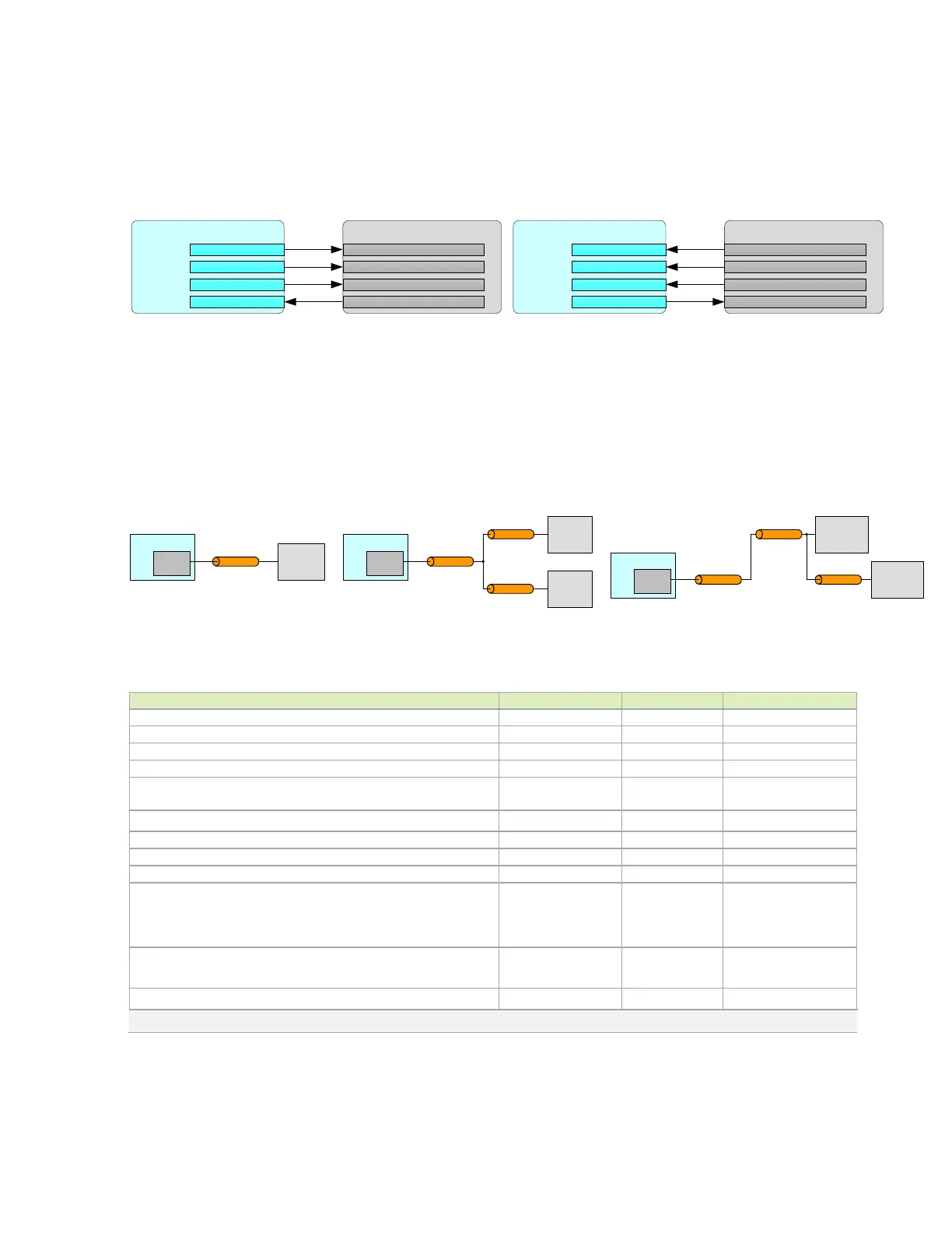
Figure 12-3 shows the basic connections used.
Figure 12-3. Basic SPI Initiator and Target Connections
Jetson Initiator
SPIn_CSx
SP In_SCK
SP In_MOSI
SP In_MISO
SPI Target Device
CS (Chip Select)
CLK ( Clock)
MOSI (Initiator out, Target in)
MISO (Initiator in, Target out)
Jetson Target
SPIn_CSx
SP In_SCK
SP In_MOSI
SP In_MISO
SPI Initiator Device
CS (Chip Select)
CLK ( Clock)
MOSI (Initiator out, Target in)
MISO (Initiator in, Target out)
12.2.1 SPI Design Guidelines
The following guidelines meet the SPI design guidelines.
Figure 12-4. SPI Topologies
Jetson
SPI
Device
#1
Main trunk
SPI
Device
#2
SPI
Device
#1
Main trunk
SPI
Device
#2
Branch-A
Branch-B
Branch-A
Branch-B
2x-Load Star Topology 2x-Load Daisy Topology
SPI
Device
Main trunk
SoC
Jetson
SoC
Jetson
SoC
Point-Point Topology
Table 12-5. SPI Interface Signal Routing Requirements
Configuration / device organization
Max loading (total of all loads)
Breakout region impedance
Minimum width
and spacing
Via proximity (signal to reference)
Trace spacing: Microstrip / Stripline
Max trace length/delay (PCB main trunk) For MOSI, MISO, SCK
and CS
Point-point
195 (1228)
120 (756)
mm (ps)
Max trace length/delay (Branch-A) for MOSI, MISO, SCK and CS
2x-load star/daisy
75 (472)
Max trace length/delay skew from MOSI, MISO and CS to SCK
: Up to four signal vias can share a single GND return via

 Loading...


