SD Card and SDIO
NVIDIA Jetson Xavier NX DG-09693-001_v1.7 | 62
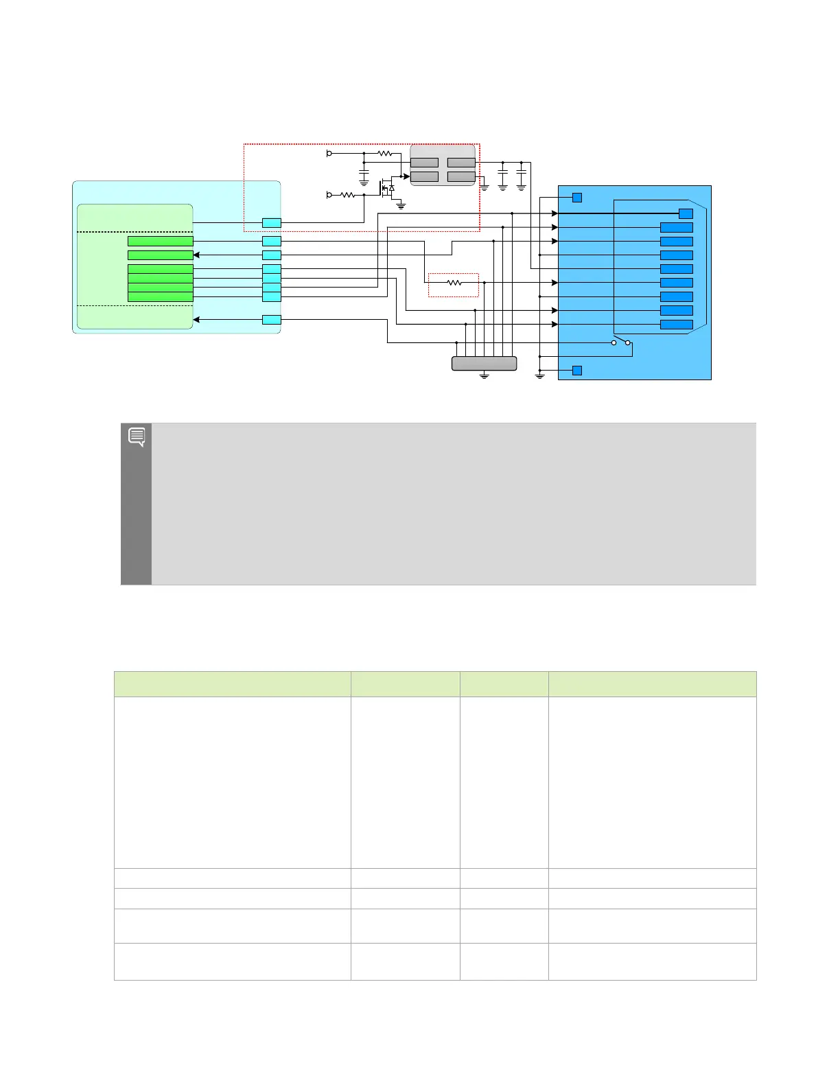
Figure 10-1. SD Card Connection Example
ESD
DATA2
DATA3
CMD
VDD
CLK
GND
DATA0
DATA1
C_DETECT
COMMON
VDD_3V3_SYS
Load S witch
VO UTVIN
GND
0Ω
Jetson
SoC
SDMMC3
SDMMC3_ CLK
SDMMC3_ CMD
SDMMC3_ DAT3
GP IO
SDMMC_CLK
SDMMC_CMD
SDMMC_DAT0
SDMMC_DAT1
SDMMC_DAT2
SDMMC_DAT3
GP IO
SDMMC3_ DAT2
SDMMC3_ DAT1
SDMMC3_ DAT0
227
229
#
219
221
223
225
0.1uF 10uF
ON
0.1uF
GND
SDMMC_CD
See Note 3
2. 2kΩ
VDD_1V8
G
S
D
2. 2kΩ
#
See Note 1
See Note 2
Notes:
1. The supply or load switch for the SD Card VDD must be enabled with a GPIO from Jetson. This
is required for correct operation after a warm boot. The GPIO used should be selected so VDD
is not powered on by default.
2. The supply (regulator, load switch, etc.) used to supply the SD Card VDD rail should be current
limited if the supply is shorted to GND.
3. Having 0Ω, 0402 resistor is recommended in case of issues with EMI where it can be replaced
with an appropriate device.
Table 10-2. SD Card and SDIO Interface Signal Routing Requirements
Max frequency
3.3V Signaling
DS
HS
1.8V Signaling
SDR12
SDR25
SDR50
SDR104
DDR50
25 (12.5)
50 (25)
25 (12.5)
50 (25)
100 (50)
208 (104)
50 (50)
MHz (MB/s)
See Note 1
Topology Point to point
Reference plane
or
Trace impedance 50
±15%. 45Ω optional depending on
stack-up
Max via count
PTH
4
Independent of stack-up layers.
Depends on stack-up layers.

 Loading...


