USB and PCIe
NVIDIA Jetson Xavier NX DG-09693-001_v1.7 | 23
0.1uF recommended. Only required for TX
pair when routed to connector
Location (max length to adjacent
discontinuity)
Discontinuity is connector, via, or
component pad
GND/PWR void under/above cap is
preferred
Voiding is required if AC cap size is 0603
or larger
ESD (On-chip protection diode can withstand 2kV HMM. External ESD is optional. Designs should include ESD footprint as a
stuffing option)
Max Junction capacitance (IO to GND)
GEN1
0.8
pF
GEN1: SEMTECH RClamp0524p
GEN2: TPD4E02B04DQA
Pad should be on the net – not trace
stub
Location (max length to adjacent
discontinuity)
Discontinuity is connector, via, or
component pad
Common-mode Choke
(Not recommended – only used if absolutely required for EMI issues). See Chapter 18 for details on CMC if implemented.
FPC (Additional length of Flexible Printed Circuit Board)
The FPC routing should be included for PCB trace calculations (max length, etc.)
Strongly recommend being the same
as the PCB or better
If worse than PCB, the PCB and FPC
length must be re-estimated
SMT Connector GND Voiding
GND plane under signal pad should be voided. Size of void should be the same
size as the pad.
Connector used must be USB-IF certified
General: See Chapter 18 for guidelines related to serpentine routing, routing over voids and noise coupling
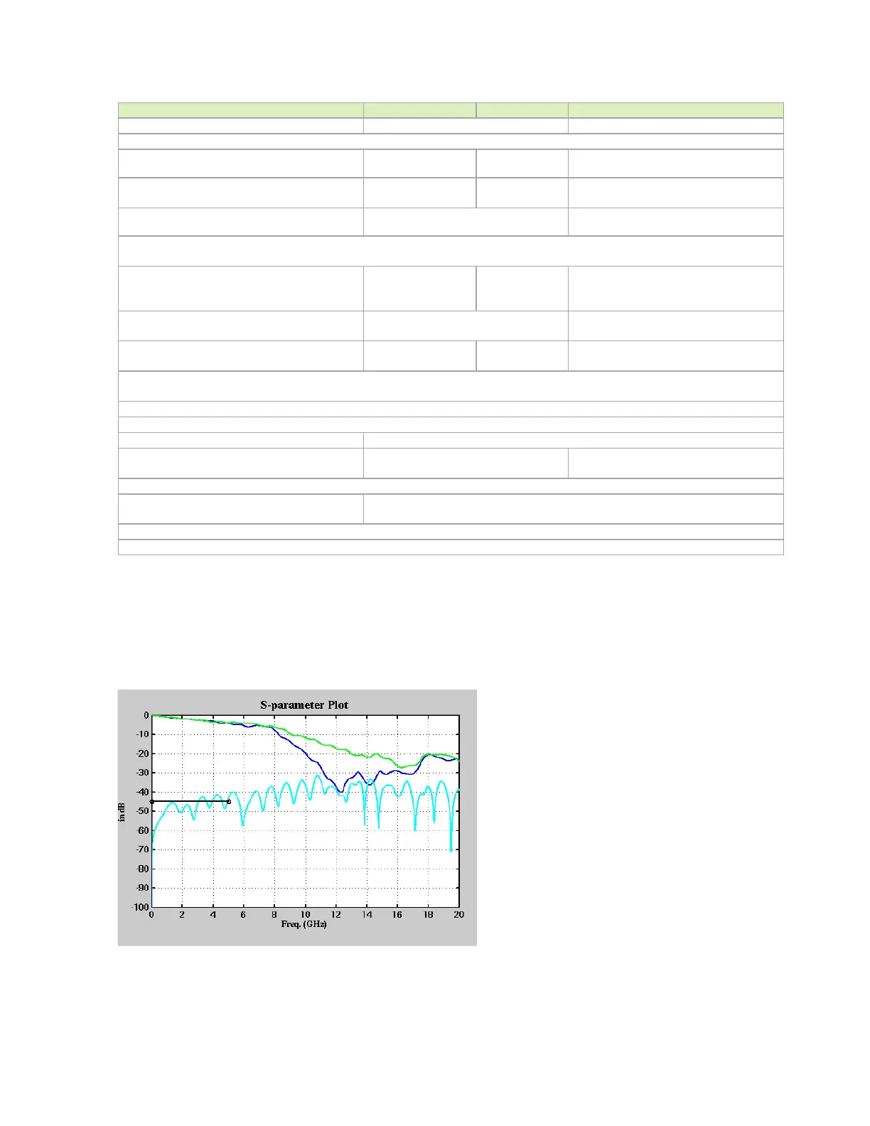
The following figures show the USB 3.2. Interface signal routing requirements.
Figure 6-3. IL/NEXT Plot (GEN1)

 Loading...


