Display
NVIDIA Jetson Xavier NX DG-09693-001_v1.7 | 43
Value 0.1 uF Discrete 0402
Max distance from AC cap to connector
RBR/HBR
HBR2/HBR3
No requirement
0.5
in
Voiding
RBR/HBR
HBR2/HBR3
No requirement
Voiding required
: Voiding the plane directly under
the pad 3-4 mils larger than the pad
size is recommended.
Voiding
RBR/HBR
HBR2/HBR3
No requirement
Voiding required
Standard DP connector: Voiding
requirement is stack-up dependent. For
typical stack-ups, voiding on the layer
under the connector pad is required to
be 5.7 mil larger than the connector
pad.
General: See Chapter 18 for guidelines related to Serpentine routing, routing over voids and noise coupling
Notes:
1. For eDP/DP, the spec puts a higher priority on the trace loss characteristic than on the impedance. However, before selecting
85Ω for impedance, it is important to make sure the selected stack-up, material and trace dimension can achieve the needed
low loss characteristic.
2. Longer trace lengths may be possible if the total trace loss is equal to or better than the target. If the loss is greater, the max
trace lengths will need to be reduced.
3. Do not perform length matching within breakout region. Recommend doing trace length matching to <1ps before vias or any
discontinuity to minimize common mode conversion.
4. The average of the differential signals is used for length matching.
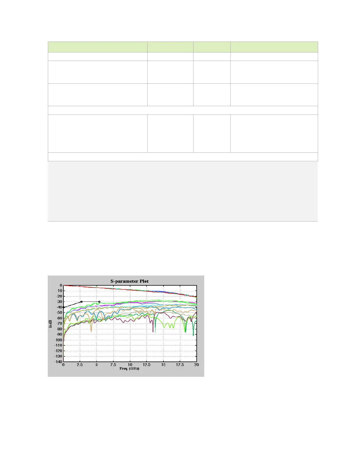
The following figures show the eDP and DP interface signal routing requirements.
Figure 8-3. S-Parameter (up to HBR2)

 Loading...


