Display
NVIDIA Jetson Xavier NX DG-09693-001_v1.7 | 40
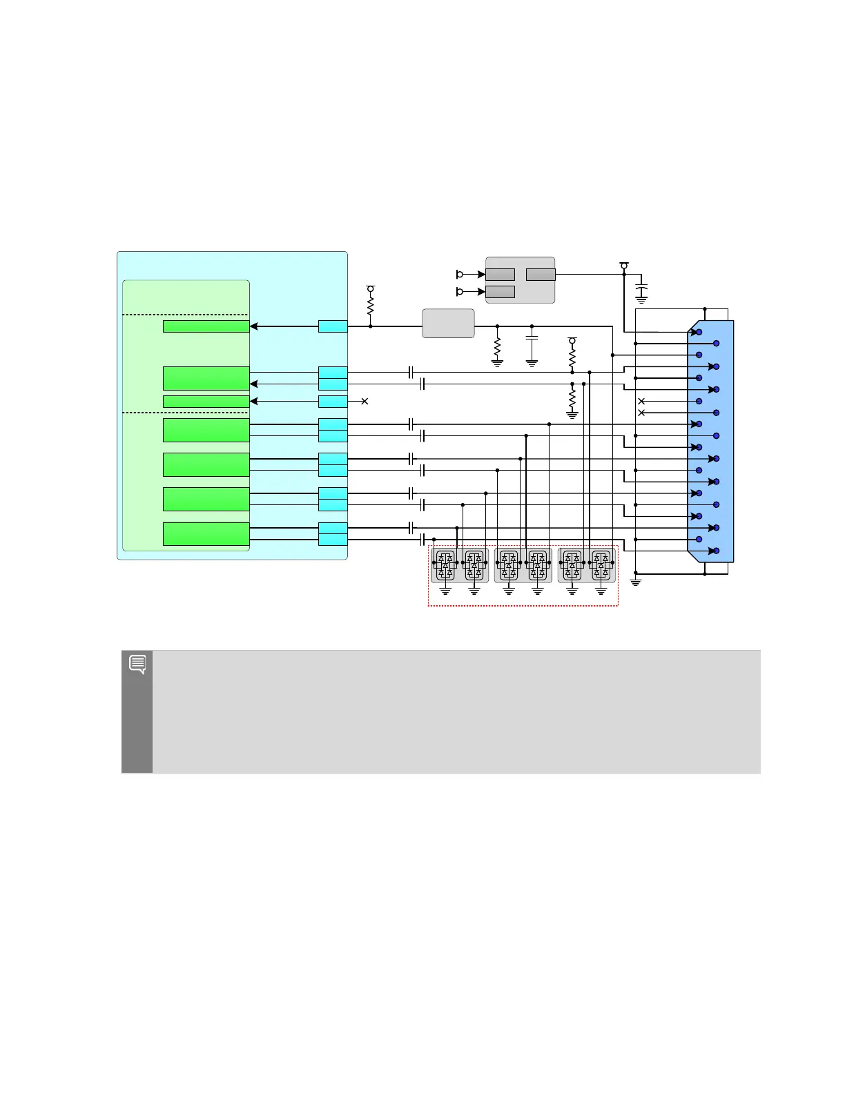
8.1 eDP and DP
Figure 8-1 shows the DP and eDP connection example.
Figure 8-1. DP and eDP Connection Example
0. 1uF
0. 1uF
0. 1uF
0. 1uF
0. 1uF
0. 1uF
0. 1uF
0. 1uF
0. 1uF
0. 1uF
10 0kΩ
VDD_3V3_SY S
10 0kΩ
VDD_3V3_EDP
DP
Conn
.
PWR
PWR_RET
HPD
AUXN
GND
AUXP
CEC_DP
MODE
LANE _3 N
GND
LANE _3 P
LANE _2 N
GND
LANE _2 P
LANE _1 N
GND
LANE _1 P
LANE _0 N
GND
LANE _0 P
1
3
5
11
7
9
13
15
17
19
2
10
12
6
8
14
16
18
4
20
T PD4E 05U06
Jetson
SoC – HDMI/DP
HDMI_DPx_TXDP3
HDMI_Dx_TXDN3
HDMI_DPx_TXDP2
HDMI_DPx_TXDN2
HDMI_DPx_TXDP1
HDMI_DPx_TXDN1
HDMI_DPx_TXDP0
HDMI_DPx_TXDN0
DP_AUX_CHx_N
DP_AUX_CHx_P
DP_AUX_CHx_HPD
DP
HDMI
HDMI_CEC
DPx_HPD
DPx_AUX_N
DPx_AUX_P
HDMI_CEC
DPx_TXD3_N
DPx_TXD3_P
DPx_TXD2_N
DPx_TXD2_P
DPx_TXD1_N
DPx_TXD1_P
DPx_TXD0_N
DPx_TXD0_P
88/96
92/100
90/98
94
41/65
39/63
47/71
45/69
53/77
59/83
57/81
51/75
0. 1uF
VDD_3V3_SY S
3V 3_ IO_ PG
VDD_1V8
10 kΩ
Load Switch
EN
IN OUT
Lev el Shifte r
1.8V 3.3V
0/1
10 kΩ
Notes:
1. Level shifter required on DP0_HPD to avoid the pin from being driven when Jetson Xavier NX
is off. The level shifter must be non-inverting (preserve the polarity of the HPD signal from the
display). The reference design uses a BJT level shifter and a resistor divider is needed. See
the reference design if a similar approach will be used.
2. Load Switch enable is from powergood pin of main 3.3V supply.

 Loading...


