USB and PCIe
NVIDIA Jetson Xavier NX DG-09693-001_v1.7 | 25
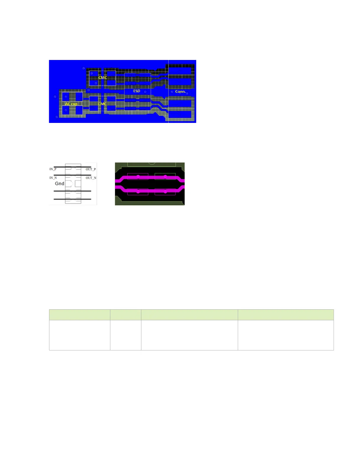
Figure 6-7. Component Placement
Figure 6-8. ESD Layout Recommendations
6.1.2.1 Common USB Routing Guidelines
If routing to USB device or USB connector includes a flex or 2nd PCB, the total routing
including all PCBs/flexes must be used for the max trace and skew calculations.
Keep critical USB related traces away from other signal traces or unrelated power
traces/areas or power supply components
Table 6-6. USB 2.0 Signal Connections
USB[2:0]_D_P
USB[2:0]_D_N
DIFF I/O If used, 90Ω common-mode chokes
close to connector. ESD Protection
between choke and connector on each
line to GND
USB Differential Data Pair: Connect
to USB connector, Mini-Card socket,
hub or another device on the PCB.

 Loading...


