USB and PCIe
NVIDIA Jetson Xavier NX DG-09693-001_v1.7 | 33
20%, 0402 X5R or better. Only required
for TX pair when routed to connector.
Voiding the plane directly under the
pad 3-4 mils larger than the pad size
Remove unwanted GND fill that is either floating or act like antenna
Void all layers of golden finger area
under the pad 5.7 mils larger than
the pad size is recommended.
General: See Chapter 18 for guidelines related to serpentine routing, routing over voids and noise coupling
Notes:
1. The PCIe spec. has 40-60Ω absolute min/max trace impedance, which can be used instead of the 50Ω, ± 15%.
2. If routing in the same layer is necessary, route group TX and RX separately without mixing RX/TX routes and keep distance
between nearest TX/RX trace and RX to other signals 3x RX-RX separation.
3. The average of the differential signals is used for length matching.
4. Do length matching before Via transitions to different layers or any discontinuity to minimize common mode conversion.
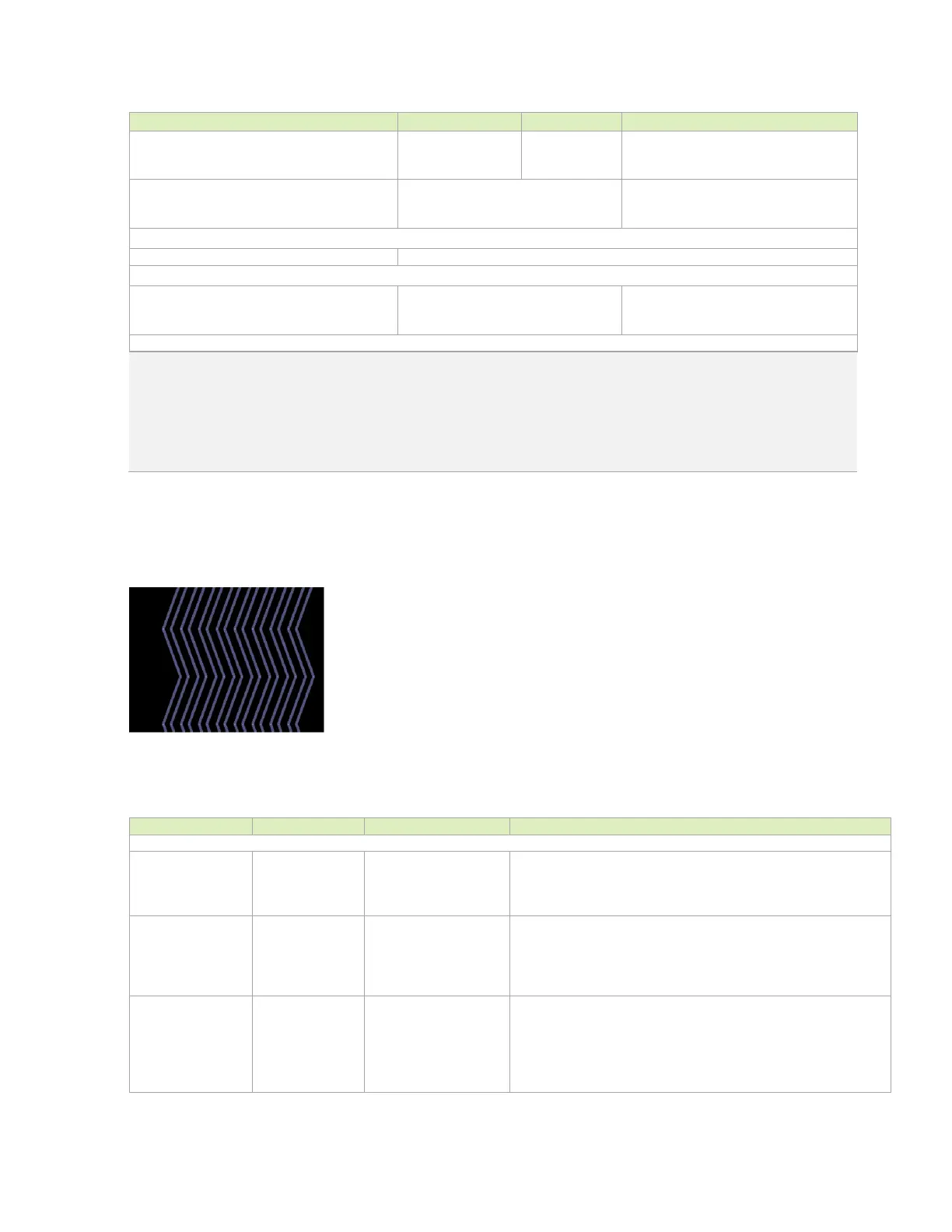
Figure 6-15. Example Zig-Zag Routing
Table 6-11. PCIe Signal Connections
PCIe Interface 0 (x4 – Controller #5)
PCIE0_TX3_N/P
PCIE0_TX2_N/P
PCIE0_TX1_N/P
PCIE0_TX0_N/P
Capacitor
Differential Transmit Data Pairs: Connect to TX_N/P pins of PCIe
connector or RX_N/P pin of PCIe device through AC cap according
to supported configuration.
PCIE0_RX3_N/P
PCIE0_RX2_N/P
PCIE0_RX1_N/P
PCIE0_RX0_N/P
capacitors near Jetson
Xavier NX pins or
device if device on
Differential Receive Data Pairs: Connect to RX_N/P pins of PCIe
connector or TX_N/P pin of PCIe device through AC cap according
to supported configuration.
(Rootport)
DIFF IN
(Endpoint)
Differential Reference Clock Output: Connected to a mux on the
module that selects either PEX_CLK5 or NVHS0_REFCLK.
Connect to REFCLK_N/P pins of PCIe device/connector. For Root
Port operation, set the mux to select PEX_CLK5 (CAN0_EN = 0).
For Endpoint, set the mux to select NVHS0_REFCLK (CAN_EN =

 Loading...


