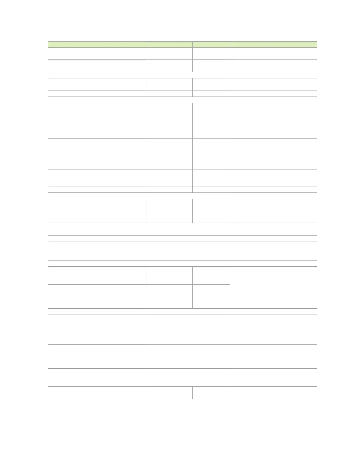
USB and PCIe
NVIDIA Jetson Xavier NX DG-09693-001_v1.7 | 22
@ Tr = 200ps (10%-90%)
@ Tr = 61ps (10%-90%)
Near End Crosstalk (NEXT)
DC – 5GHz per each TX-RX NEXT. See
(See Figure 6-3) and Figure 6-4)
Trace Impedance: Diff pair / Single Ended
±15%. Intrinsic Zdf, does not account
for coupling from other trace pairs
Trace loss characteristic (max):
GEN1
GEN2
0.7
0.9
dB/in @ 2.5GHz
dB/in @ 5GHz
The following max length is derived
based on this characteristic. The length
constraint must be re-defined if loss
characteristic is changed. The trace
loss profile for Gen2 support is based
on the dielectric material EM370(5).
Breakout Region – Max length
Minimum trace width and spacing
GEN1 (Host)
152 (1014)
Max Trace Length (Device) GEN1 only
Max Intra-Pair Skew (RX/TX_N to RX/TX_P)
Do not perform length matching within
breakout region. Trace length matching
should be done before discontinuities.
Differential pair uncoupled length
Trace Spacing for TX/RX Interleaving
Trace Spacing: Microstrip / Stripline
Pair-Pair
To Ref plane and SMT pad
To unrelated high-speed signals
4x / 3x
4x / 3x
Dielectric
height
Trace Spacing for TX/RX Non-interleaving
TX-RX Xtalk is very critical in PCB trace routing. The ideal solution is to route TX and RX on different layers.
If routing on the same layer, strongly recommend not interleaving TX and RX lanes
If have to have interleaving routing in breakout, all the inter-pair spacing should follow the rule of inter-S
NEXT
(between TX/RX pair
spacing)
The breakout trace width is suggested to be the minimum to increase inter-pair spacing
Do not perform serpentine routing for intra-pair skew compensation in the breakout region
NEXT
Breakout
4.85x
Dielectric
This is the recommended dimensions
for meeting the NEXT requirement.
Stripline structure in a GSSG structure
is assumed (holds in broadside-coupled
stripline structure)
Breakout
Main-route
11
Max trace length -
BRK
mm
Keep symmetry
Y-pattern helps with Xtalk suppression.
It can also reduce the limit of the pair-
pair distance. Review needed
(NEXT/FEXT check) if via placement
does not use Y-pattern. See Figure 6-5.
Place GND via as symmetrically as
possible to data pair vias. Up to 4
signal vias (2 diff pairs) can share a
GND via is used to maintain return
path, while its Xtalk suppression is
limited
PTH vias
4 if all vias are PTH via
Not limited as long as total channel loss meets IL spec
long via stub requires review (IL and
resonance dip check)
Additional Component Placement Order
Chip AC capacitor (TX only) common mode choke ESD Connector

 Loading...


