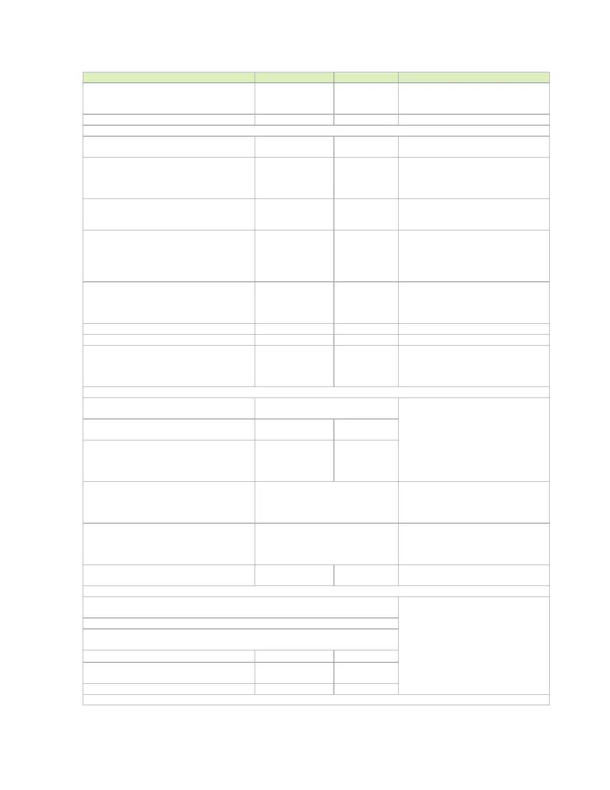
Display
NVIDIA Jetson Xavier NX DG-09693-001_v1.7 | 48
Trace impedance: Diff pair
±10%. Target is 100Ω. 95Ω for the
breakout and main route is an
Trace spacing/Length/Skew
Trace loss characteristic:
dB/in. @ 3GHz
dB/in. @ 1.5GHz
The max length is derived based on this
characteristic. See Note 1.
Trace spacing (pair-pair)
Stripline
Microstrip: pre 1.4b
3x
4x
dielectric
For Stripline, this is 3x of the thinner of
above and below.
Trace spacing (Main link to DDC)
Stripline
3x
dielectric
For Stripline, this is 3x of the thinner of
above and below.
Max total length/delay (1.4b/2.0 - up to
5.94Gbps)
Stripline
Microstrip (5x spacing)
100 (690)
90 (531)
mm (ps)
Propagation delay: 175ps/in. for stripline,
150ps/in. for microstrip). Stripline is
preferred.
Max Total Length/Delay (Pre-1.4b - (up to
165Mhz)
Microstrip Stripline
254 (1500)
mm (ps)
Propagation delay: 175ps/in. for stripline,
150ps/in. for microstrip).
Max intra-pair (within pair) skew
Max inter-pair (pair to pair) skew
Max GND transition via distance
For signals switching reference layers,
add one or two ground stitching vias. It is
recommended they be symmetrical to
- Y-pattern is recommended
- keep symmetry
Xtalk suppression is the best by Y-
pattern. Also it can reduce the limit of
pair-pair distance. Need review
(NEXT/FEXT check) if via placement is
not Y-pattern. See
Figure 8-11
Recommended via dimension
drill/pad
Antipad
200/400
840
uM
Place GND via as symmetrically as
possible to data pair vias. Up to four
signal vias (2 diff pairs) can share a
GND via is used to maintain return path,
while its Xtalk suppression is limited
PTH via
u-via
2 if all vias are PTH via
Not limited if total channel loss
long via stub requires review (IL and
resonance dip check)
The main route via dimensions should comply with the via structure rules (See via
section)
See topology in Figure 8-8
For the connector pin vias, follow the rules for the connector pin vias (See via section)
The traces after main route via should be routed as 100Ω differential or as uncoupled
50ohm SE traces on PCB top or bottom.
PD
Max distance from AC cap to RPD stubbing
point (seg A)
Max distance between ESD and signal via

 Loading...


