RL78/G13 CHAPTER 3 CPU ARCHITECTURE
R01UH0146EJ0100 Rev.1.00 123
Sep 22, 2011
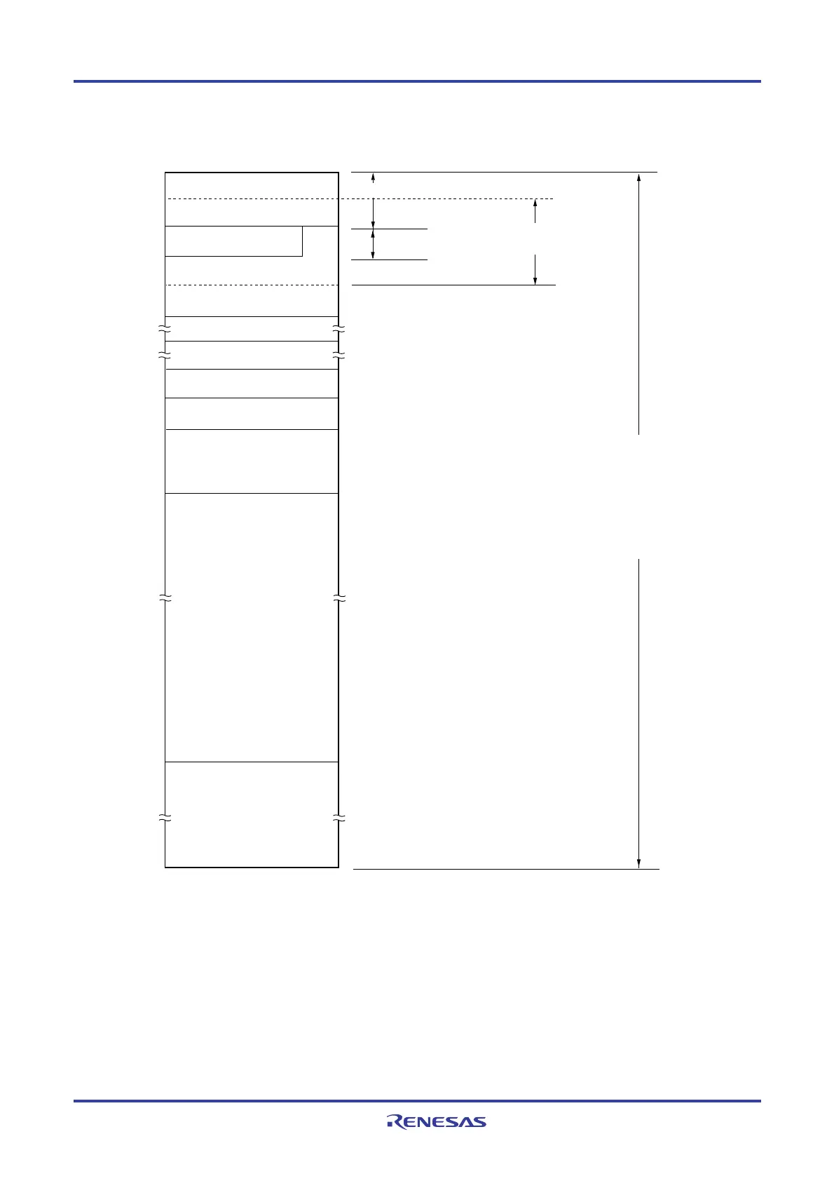
Figure 3-14. Correspondence Between Data Memory and Addressing
(R5F100xD, R5F101xD(x = 6 to 8, A to C, E to G, J, L))
00000H
EFFFFH
F0000H
F0FFFH
F1000H
FF300H
FF2FFH
FFEDFH
FFEE0H
FFEFFH
FFF00H
FFFFFH
0BFFFH
0C000H
F07FFH
F0800H
Special function register (SFR)
256 bytes
General-purpose register
32 bytes
RAM
Note 1
3 KB
Mirror
40 KB
Reserved
Special function register (2nd SFR)
2 KB
Reserved
Code flash memory
48 KB
Direct addressing
Register indirect addressing
Based addressing
Based indexed addressing
Short direct
addressing
SFR addressing
Register addressing
FFF1FH
FFF20H
FFE1FH
FFE20H
Data flash memory
Note 2
4 KB
F1FFFH
F2000H
Reserved
FC000H
FBFFFH
Notes 1. Use of the area FF300H to FF309H is prohibited when using the self-programming function and data flash
function, because this area is used for self-programming library.
2. R5F100xD only.
Caution When executing instructions from the RAM area while RAM parity error resets are enabled (RPERDIS
= 1), be sure to initialize the used RAM area + 10 bytes.
<R>
<R>

 Loading...


