RL78/G13 CHAPTER 11 A/D CONVERTER
R01UH0146EJ0100 Rev.1.00 487
Sep 22, 2011
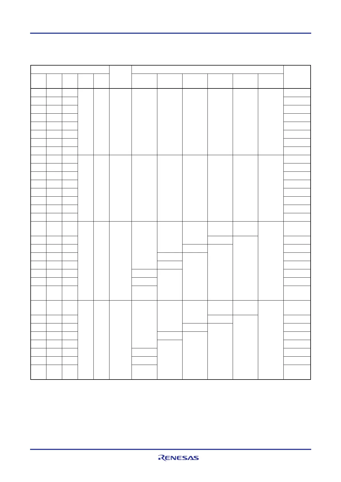
Table 11-3. A/D Conversion Time Selection (4/8)
(4) 1.6 V ≤ VDD < 2.7 V when there is no stabilization wait time (software trigger mode/hardware trigger no-wait mode)
A/D Converter Mode Register 0 (ADM0)
Conversion Time Selection
FR2 FR1 FR0 LV1 LV0
Mode
fCLK = 1
MHz
fCLK = 2
MHz
fCLK = 4
MHz
fCLK = 8
MHz
Note 1
fCLK = 16
MHz
Note 2
f
CLK = 32
MHz
Conversion
Clock (f
AD)
0 0 0 fCLK/64
0 0 1 fCLK/32
0 1 0 fCLK/16
0 1 1 fCLK/8
1 0 0 fCLK/6
1 0 1 fCLK/5
1 1 0 fCLK/4
1 1 1
0 0 Normal 1
Setting
prohibited
Setting
prohibited
Setting
prohibited
Setting
prohibited
Setting
prohibited
Setting
prohibited
f
CLK/2
0 0 0 fCLK/64
0 0 1 fCLK/32
0 1 0 fCLK/16
0 1 1 fCLK/8
1 0 0 fCLK/6
1 0 1 fCLK/5
1 1 0 fCLK/4
1 1 1
0 1 Normal 2
Setting
prohibited
Setting
prohibited
Setting
prohibited
Setting
prohibited
Setting
prohibited
Setting
prohibited
f
CLK/2
0 0 0
Setting
prohibited
76
μ
s fCLK/64
0 0 1
Setting
prohibited
76
μ
s fCLK/32
0 1 0
Setting
prohibited
76
μ
s fCLK/16
0 1 1 76
μ
s fCLK/8
1 0 0
Setting
prohibited
57
μ
s fCLK/6
1 0 1 95
μ
s fCLK/5
1 1 0 76
μ
s fCLK/4
1 1 1
1 0 Low-
voltage 1
Setting
prohibited
Setting
prohibited
Setting
prohibited
Setting
prohibited
Setting
prohibited
Setting
prohibited
f
CLK/2
0 0 0
Setting
prohibited
68
μ
s fCLK/64
0 0 1
Setting
prohibited
68
μ
s fCLK/32
0 1 0
Setting
prohibited
68
μ
s fCLK/16
0 1 1 68
μ
s fCLK/8
1 0 0
Setting
prohibited
fCLK/6
1 0 1 85
μ
s fCLK/5
1 1 0 68
μ
s fCLK/4
1 1 1
1 1 Low-
voltage 2
Setting
prohibited
Setting
prohibited
Setting
prohibited
Setting
prohibited
Setting
prohibited
Setting
prohibited
f
CLK/2
Notes 1. Setting is prohibited when VDD < 1.8 V.
2. Setting is prohibited when VDD < 2.4 V.
Cautions 1. When rewriting the FR2 to FR0, LV1, and LV0 bits to other than the same data, stop A/D conversion
once (ADCS = 0) beforehand.
2. The above conversion time does not include clock frequency errors. Select conversion time, taking
clock frequency errors into consideration.
Remark f
CLK: CPU/peripheral hardware clock frequency
<R>

 Loading...


