RL78/G13 CHAPTER 11 A/D CONVERTER
R01UH0146EJ0100 Rev.1.00 492
Sep 22, 2011
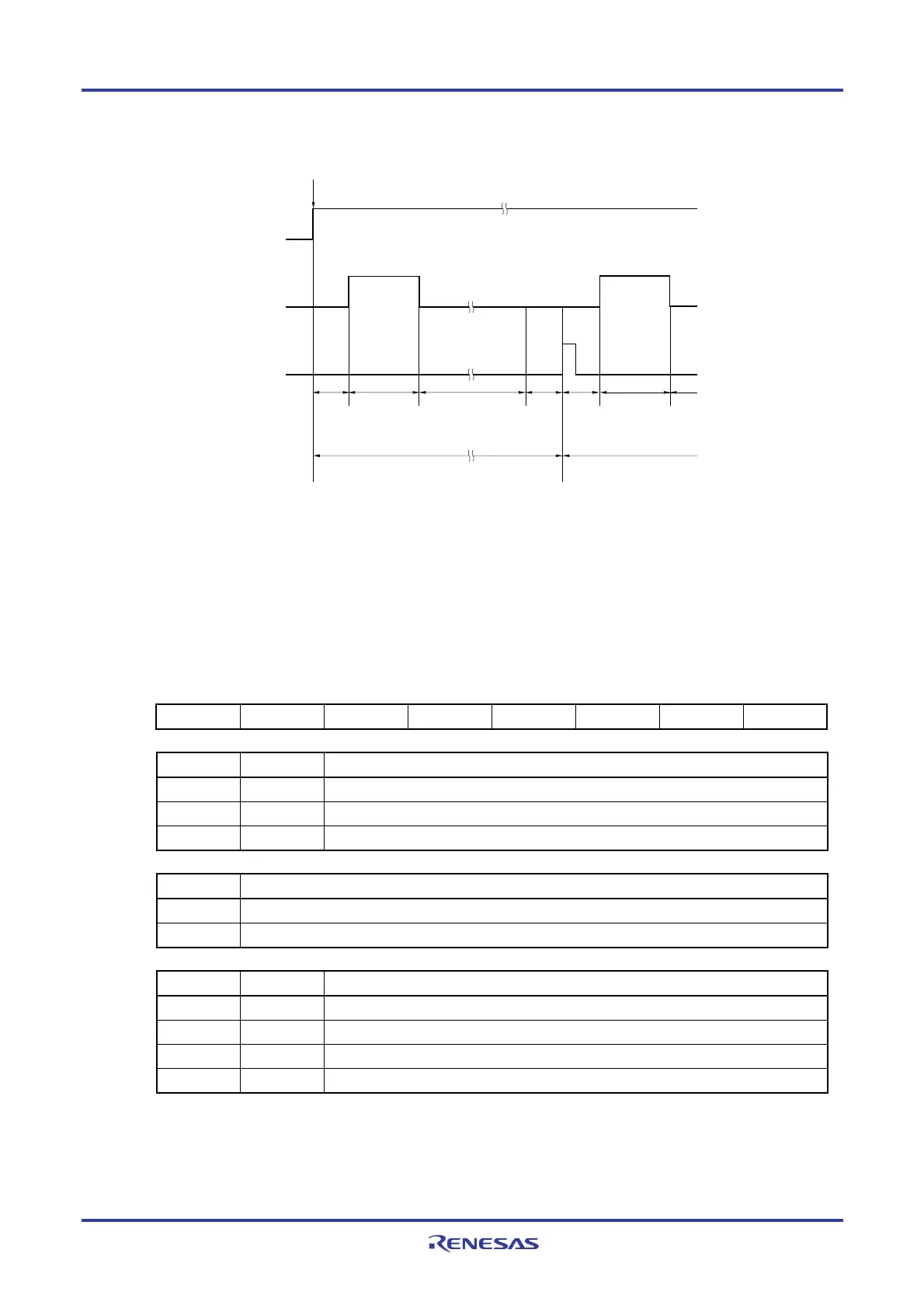
Figure 11-5. A/D Converter Sampling and A/D Conversion Timing (Example for Software Trigger Mode)
ADCS
Conversion time Conversion time
Sampling
Sampling
timing
INTAD
ADCS ← 1 or ADS rewrite
Sampling
SAR
clear
SAR
clear
Transfer
to ADCR,
INTAD
generation
Successive conversion
(3) A/D converter mode register 1 (ADM1)
This register is used to specify the A/D conversion trigger, conversion mode, and hardware trigger signal.
The ADM1 register can be set by a 1-bit or 8-bit memory manipulation instruction.
Reset signal generation clears this register to 00H.
Figure 11-6. Format of A/D Converter Mode Register 1 (ADM1)
Address: FFF32H After reset: 00H R/W
Symbol 7 6 5 4 3 2 1 0
ADM1 ADTMD1 ADTMD0 ADSCM 0 0 0 ADTRS1 ADTRS0
ADTMD1 ADTMD0 Selection of the A/D conversion trigger mode
0
−
Software trigger mode
1 0 Hardware trigger no-wait mode
1 1 Hardware trigger wait mode
ADSCM Specification of the A/D conversion mode
0 Sequential conversion mode
1 One-shot conversion mode
ADTRS1 ADTRS0 Selection of the hardware trigger signal
0 0 End of timer channel 1 count or capture interrupt signal (INTTM01)
0 1 Setting prohibited
1 0 Real-time clock interrupt signal (INTRTC)
1 1 Interval timer interrupt signal (INTIT)
Cautions 1. Only rewrite the value of the ADM1 register while conversion operation is stopped (which is
indicated by the ADCS bit of A/D converter mode register 0 (ADM0) being 0).
2. For the trigger interval in the hardware trigger wait mode, specify at least “A/D Conversion
Time, When there is stabilization wait time” described in Table 11-3.

 Loading...


