RL78/G13 CHAPTER 11 A/D CONVERTER
R01UH0146EJ0100 Rev.1.00 493
Sep 22, 2011
(4) A/D converter mode register 2 (ADM2)
This register is used to select the A/D converter reference voltage, check the upper limit and lower limit A/D
conversion result values, select the resolution, and specify whether to use the SNOOZE mode.
The ADM2 register can be set by a 1-bit or 8-bit memory manipulation instruction.
Reset signal generation clears this register to 00H.
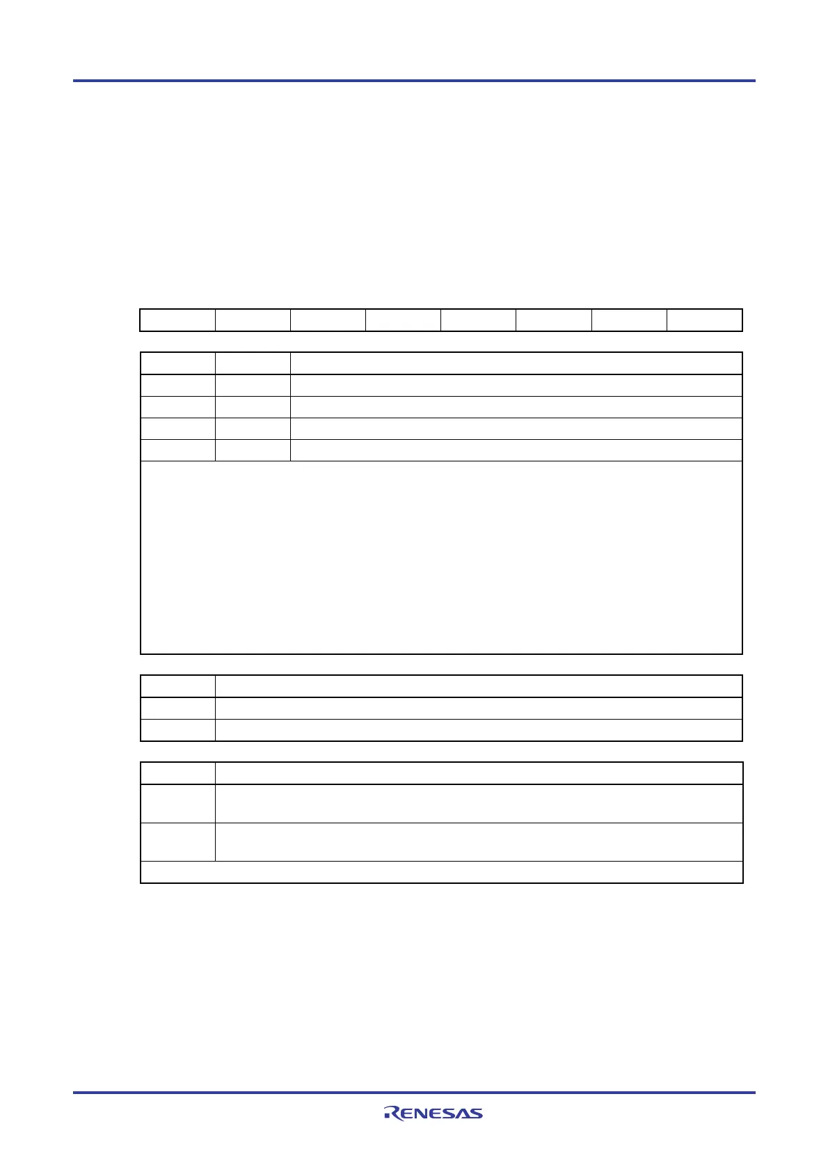
Figure 11-7. Format of A/D Converter Mode Register 2 (ADM2) (1/2)
Address: F0010H After reset: 00H R/W
Symbol 7 6 5 4 <3> <2> 1 <0>
ADM2 ADREFP1 ADREFP0 ADREFM 0 ADRCK AWC 0 ADTYP
ADREFP1 ADREFP0 Selection of the + side reference voltage source of the A/D converter
0 0 Supplied from VDD
0 1 Supplied from P20/AVREFP/ANI0
1 0 Supplied from the internal reference voltage (1.45 V)
1 1 Setting prohibited
・ When ADREFP1 or ADREFP0 bit is rewritten, this must be configured in accordance with the following procedures.
(1) Set ADCE = 0
(2) Change the values of ADREFP1 and ADREFP0
(3) Stabilization wait time (A)
(4) Set ADCE = 1
(5) Stabilization wait time (B)
When ADREFP1 and ADREFP0 are set to 1 and 0, the setting is changed to A = 1
μ
s, B = 5
μ
s.
When ADREFP1 and ADREFP0 are set to 0 and 0 or 0 and 1, A needs no wait and B = 1
μ
s.
・ When ADREFP1 and ADREFP0 are set to 1 and 0, respectively, A/D conversion cannot be performed on the
temperature sensor output.
Be sure to perform A/D conversion while ADISS = 0.
ADREFM Selection of the − side reference voltage source of the A/D converter
0 Supplied from VSS
1 Supplied from P21/AVREFM/ANI1
ADRCK Checking the upper limit and lower limit conversion result values
0
The interrupt signal (INTAD) is output when the ADLL register ≤ the ADCR register ≤ the ADUL register
(<1>).
1
The interrupt signal (INTAD) is output when the ADCR register < the ADLL register (<2>) or the ADUL
register < the ADCR register (<3>).
Figure 11-8 shows the generation range of the interrupt signal (INTAD) for <1> to <3>.
Caution Only rewrite the value of the ADM2 register while conversion operation is stopped (which is
indicated by the ADCS bit of A/D converter mode register 0 (ADM0) being 0).
<R>
<R>
<R>

 Loading...


