RL78/G13 CHAPTER 11 A/D CONVERTER
R01UH0146EJ0100 Rev.1.00 531
Sep 22, 2011
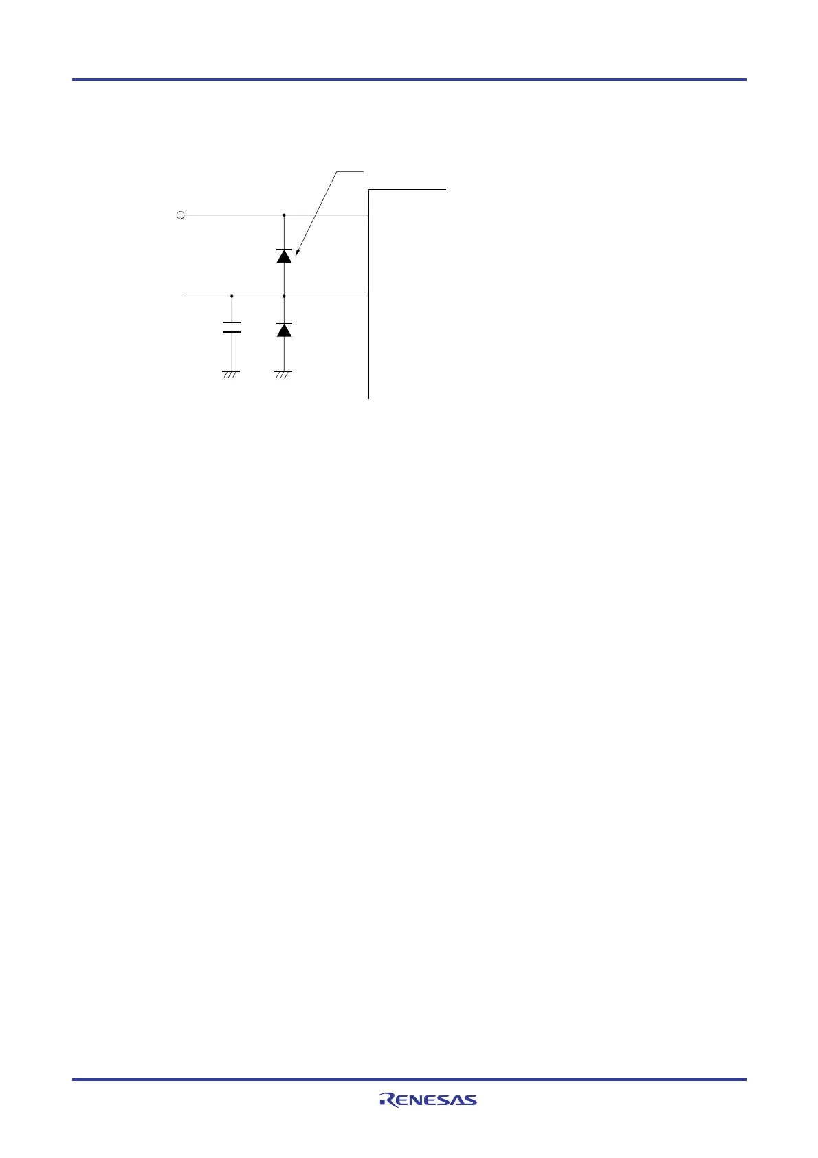
Figure 11-46. Analog Input Pin Connection
AV
REFP
or V
DD
ANI0 to ANI14, ANI16 to ANI26
Reference
voltage
input
C = 100 to 1,000 pF
If there is a possibility that noise equal to or higher than AV
REFP
and
V
DD
or equal to or lower than AV
REFM
and V
SS
may enter, clamp with
a diode with a small V
F
value (0.3 V or lower).
(5) Analog input (ANIn) pins
<1> The analog input pins (ANI0 to ANI14, ANI16 to ANI26) are also used as input port pins (P20 to P27, P00 to
P03, P35 to P37, P100, P115 to P117, P147, P120, P150 to P156).
When A/D conversion is performed with any of the ANI0 to ANI14 and ANI16 to ANI26 pins selected, do not
access P20 to P27, P00 to P03, P35 to P37, P100, P115 to P117, P147, P120, P150 to P156 while conversion
is in progress; otherwise the conversion resolution may be degraded.
<2> If a digital pulse is applied to the pins adjacent to the pins currently used for A/D conversion, the expected value
of the A/D conversion may not be obtained due to coupling noise. Therefore, do not apply a pulse to the pins
adjacent to the pin undergoing A/D conversion.
(6) Input impedance of analog input (ANIn) pins
This A/D converter charges a sampling capacitor for sampling during sampling time.
Therefore, only a leakage current flows when sampling is not in progress, and a current that charges the capacitor
flows during sampling. Consequently, the input impedance fluctuates depending on whether sampling is in progress,
and on the other states.
To make sure that sampling is effective, however, it is recommended to keep the output impedance of the analog
input source to within 1 kΩ, and to connect a capacitor of about 100 pF to the ANI0 to ANI14 and ANI16 to ANI26 pins
(see Figure 11-46).

 Loading...


