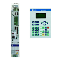
4-50 DURADRIVE HDC01.1 Drive Controller DURADRIVE Drive Controllers
DOK-DURADR-HDC01.1****-PR02-EN-P
Input circuit for sine signals G2Sin+ (A+), G2Sin- (A-):
AP5299F1.FH7
R1
R4
R2
R3
-
+
E+
E-
C2
C1
R5
Schematics
R1: N/A.
R2: N/A.
R3: N/A.
R4: N/A.
R5: 120R
C1: N/A.
C2: N/A.
Fig. 4-83: Input circuit for sine signals
Input circuit for square-wave signals G2Sin+ (A+), G2Sin- (A-):
AP5300F1.FH7
E+
E-
R5
A
B
Schematics
R5: 120R
Fig. 4-84: Input circuit for square-wave signals
Features of the differential input G2Sin+ (A+), G2Sin- (A-):
Input voltage
max. allowed amplitude encoder
signal (U
SSencoder signal
)
(1,0 + 0,2) Vss
Evaluation AD converter 12 Bit
Limit frequency 200 kHz
Input resistance 120 R
Resolution over a encoder cycle See the following note
Fig. 4-85: Features of the differential input (Sine encoder)
Note: Resolution over a period under the assumption of the following
conditions:
• Differential signal 1.0V
SS
• Reference voltage for the differential signal 2.7 V
•
ignalSSencoders
SS
12
U
V2,1
2
cycle Encoder
resolution Position
•=
Example: If U
SSencoder signal
= 1 V
SS
6826V1
V2,1
2
yclec Encoder
resolution Position
SS
SS
12
=•=
=> see also firmware functional description "Optional encoder"
(Encoder 2)
G2Sin+ (A+), G2Sin- (A-)
Sine encoder
LSA Control S.L. www.lsa-control.com comercial@lsa-control.com (+34) 960 62 43 01
 Loading...