MicroBlaze Processor Reference Guide 127
UG984 (v2018.2) June 21, 2018 www.xilinx.com
Chapter 2: MicroBlaze Architecture
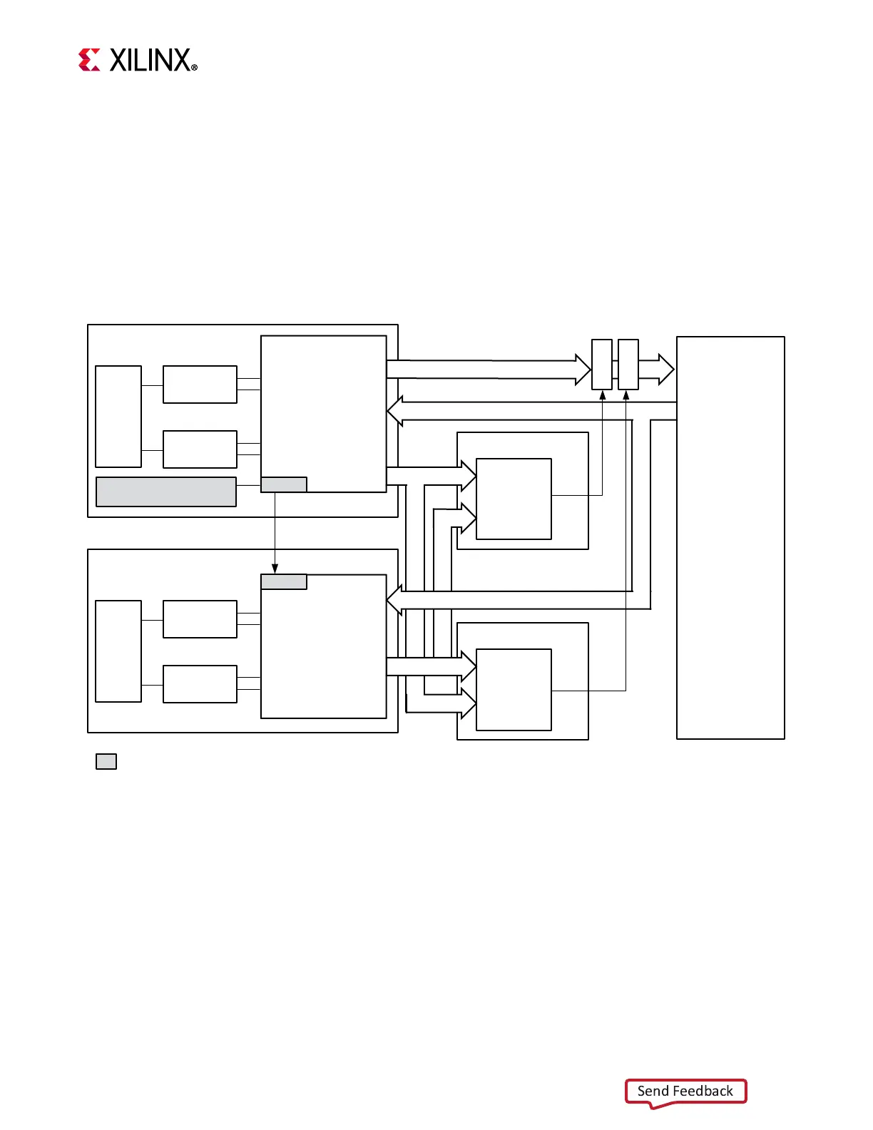
The outputs from the master MicroBlaze core drive the peripherals in the system. All data
leaving the protected area pass through inhibitors. Each inhibitor is controlled from its
associated comparator.
Each protected area of the design must be implemented in its own partition, using a
hierarchical single chip cryptography (SCC) flow. A detailed explanation of this flow, and
further references, can be found in the document Hierarchical Design Methodology Guide
(UG748)
[Ref 8].
A block diagram of the system is shown in the following figure.
Error Detection
The error detection use case requires that all transient and permanent faults are detected.
This is essential in fail safe and fault tolerant applications, where redundancy is utilized to
improve system availability.
In this system two redundant MicroBlaze processors run in lockstep. A comparator is used
to signal an error when a mis-match is detected on the outputs of the two processors. Any
error immediately causes both processors to halt, preventing further error propagation.
X-Ref Target - Figure 2-41
Figure 2-41: Lockstep Tamper Protection Application
MicroBlaze Partition
BRAM
DLMB
Bram Controller
ILMB
Bram Controller
MicroBlaze Partition
BRAM
DLMB
Bram Controller
ILMB
Bram Controller
MicroBlaze
Master
Debug
MicroBlaze
Debug Module
MicroBlaze
Slave
Debug
Comparator
I/O Interfaces
External
Memory
Interfaces
Comparator Partition
Inputs
Comparator
Comparator Partition
Inhibit
Peripheral
Partition
Inputs
Debug interface – Removed for Production
Inhibit
Outputs
C_LOCKSTEP_SLAVE=0
C_LOCKSTEP_SLAVE=1
Lockstep_Master_Out
Lockstep_Slave_In
Lockstep_Out
Lockstep_Out
X19777-091317