MicroBlaze Processor Reference Guide 155
UG984 (v2018.2) June 21, 2018 www.xilinx.com
Chapter 3: MicroBlaze Signal Interface Description
Local Memory Bus (LMB) Interface Description
The LMB is a synchronous bus used primarily to access on-chip block RAM. It uses a
minimum number of control signals and a simple protocol to ensure that local block RAM
are accessed in a single clock cycle. LMB signals and definitions are shown in the following
table. All LMB signals are active high.
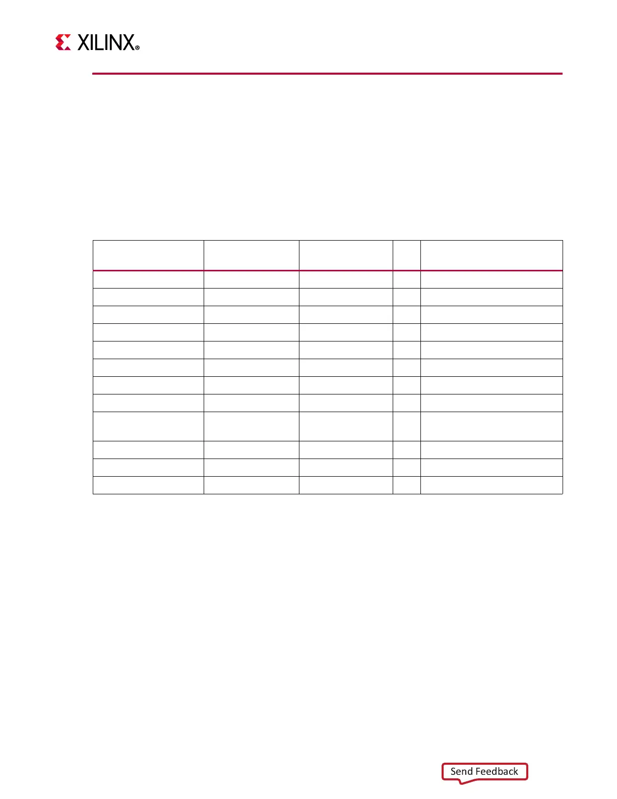
LMB Signal Interface
Addr[0:N-1]
The address bus is an output from the core and indicates the memory address that is being
accessed by the current transfer. It is valid only when
AS is high. In multicycle accesses
requiring more than one clock cycle to complete),
Addr[0:N-1] is valid only in the first
clock cycle of the transfer.
Table 3-7: LMB Bus Signals
Signal Data Interface
Instruction
Interface
Type Description
Addr[0:N-1]
1
1. N = 32 - 64, set according to parameter C_ADDR_SIZE, added in MicroBlaze v9.6.
Data_Addr[0:N-1]
1
Instr_Addr[0:N-1]
2
2. N = 32 - 64, set according to parameter C_ADDR_SIZE when PAE is enabled, added in MicroBlaze v10.0.
O
Address bus
Byte_Enable[0:3] Byte_Enable[0:3] not used
O
Byte enables
Data_Write[0:31] Data_Write[0:31] not used
O
Write data bus
AS D_AS I_AS
O
Address strobe
Read_Strobe Read_Strobe IFetch
O
Read in progress
Write_Strobe Write_Strobe not used
O
Write in progress
Data_Read[0:31] Data_Read[0:31] Instr[0:31]
I
Read data bus
Ready DReady IReady
I
Ready for next transfer
Wait
3
3. Added in LMB for MicroBlaze v8.00
DWait IWait
I
Wait until accepted transfer is
ready
CE
3
DCE ICE
I
Correctable error
UE
3
DUE IUE
I
Uncorrectable error
Clk Clk Clk
I
Bus clock